Wafer scale lens and optical system having the same

a scale lens and optical system technology, applied in the field of scale lens and optical system having the same, can solve the problems of reducing the efficiency of optical systems, requiring cameras to be small and light weight, and limited in miniaturization, so as to reduce the angle of light incident, improve diffraction efficiency, and high resolution

Inactive Publication Date: 2006-11-23
SAMSUNG ELECTRO MECHANICS CO LTD
View PDF2 Cites 80 Cited by
  • Summary
  • Abstract
  • Description
  • Claims
  • Application Information

AI Technical Summary

Benefits of technology

[0022] The present invention is characterized by a wafer scale lens in which a diffraction surface and a refractive surface are simultaneously provided on a lens substrate via replica method, calibrating chromatic difference as well as reducing the angle of the light incident onto the diffraction surface to increase diffraction efficiency and remove high order diffraction light, thereby achieving high resolution, and an optical system having the same.

Problems solved by technology

These cameras are typically required to be small and light-weight due to their characteristics.
Thus, conventional optical systems with plastic or glass lens have been used, but this is limited in miniaturization.
However, this method is limited in the thickness of polymer formed on the lens substrate, posing difficulty in realizing an efficient optical system.

Method used


Image

  • Wafer scale lens and optical system having the same
  • Wafer scale lens and optical system having the same
  • Wafer scale lens and optical system having the same

Examples


example 1

[0084] Table 1 below shows data of lens arrangement for Example 1 according to the present invention.

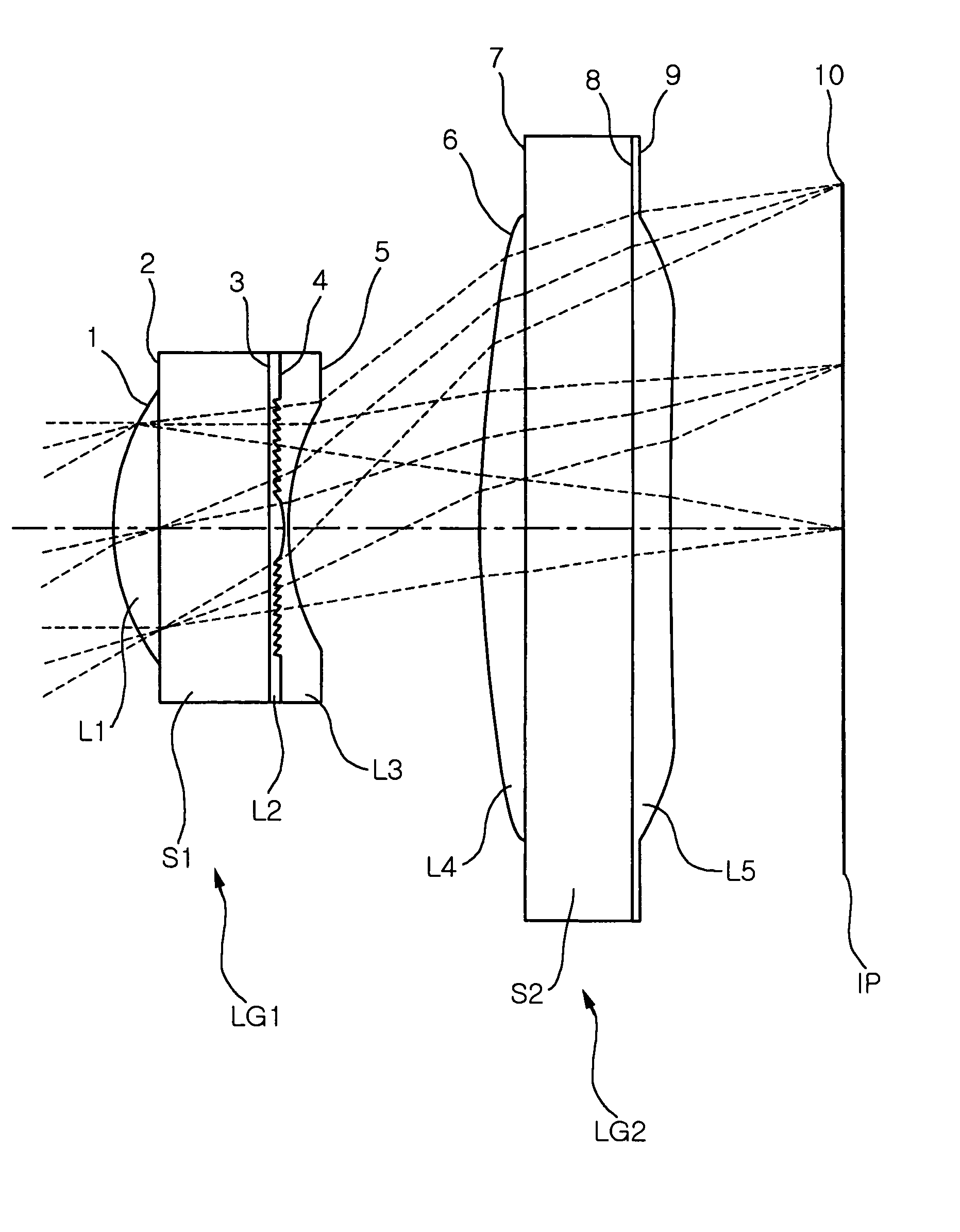
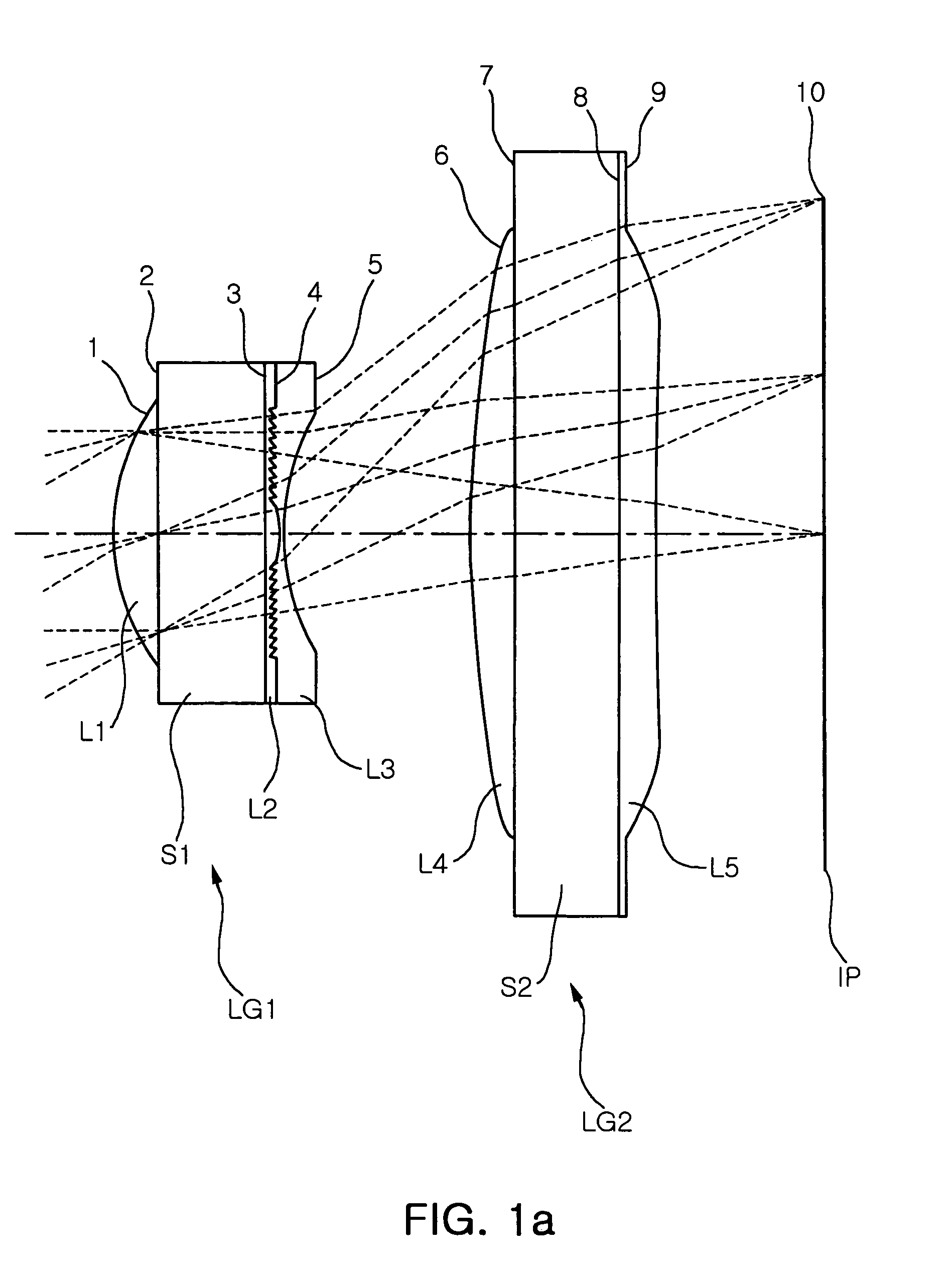
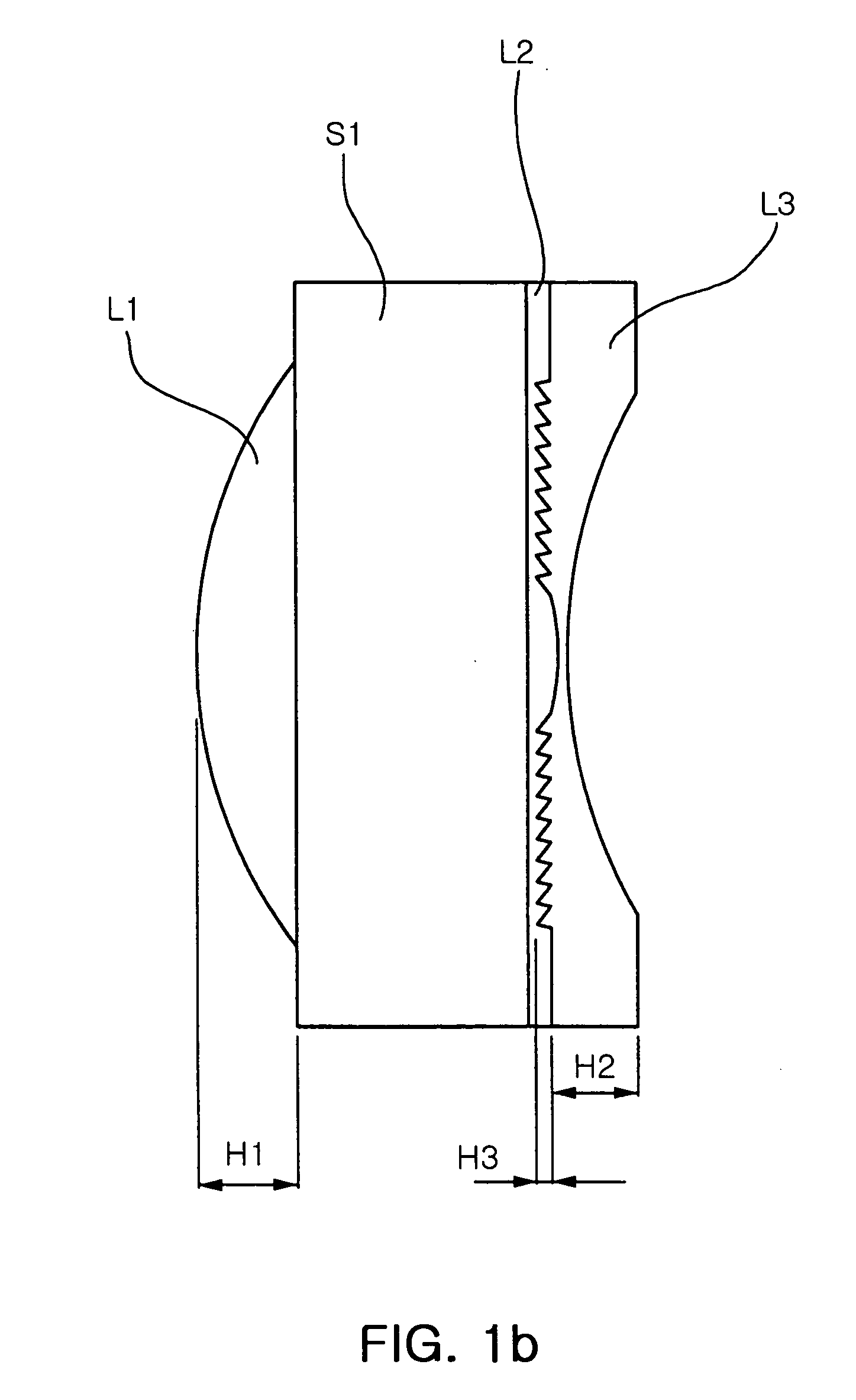
[0085]FIG. 1a is a diagram of lens arrangement in an optical system having wafer scale lenses in Example 1 of the present invention and FIG. 1b is a magnified view of the first wafer scale lens. FIGS. 2a to 2c show aberrations of the optical system of Example 1 illustrated in Table 1 and FIG. 1. FIG. 3 is a graph showing MTF characteristics of Example 1.

[0086] In addition, in the following graph illustrating astigmatism, “S” represents sagittal, and “T” represents tangential.

[0087] Here, the MTF depends on a spatial frequency of a cycle per millimeter and is defined by the following Equation 3 between a maximum intensity and a minimum intensity of light. MTF=Max-MinMax+MinEquation⁢ ⁢3

[0088] That is, if the MTF is 1, a resolution is most ideal and a resolution deteriorates as the MTF is reduced.

[0089] In Example 1, the F number FNo is 2.8, the angle of view is 60 degrees, the dis...

example 2

[0093] Table 3 below shows data of lens arrangement for Example 2 according to the present invention.

[0094]FIG. 4 is a diagram of lens arrangement in an optical system having wafer scale lenses according to the second embodiment of the present invention, and FIGS. 5a to 5c show aberrations of the optical system illustrated in Table 3 and FIG. 4. FIG. 6 is a graph illustrating MTF characteristics of the second embodiment.

[0095] In Example 2, the F number FNo is 2.8, the angle of view is 60 degrees, TL is 3.28 mm, the effective focal length f of the optical system is 2.76 mm, the focal length f1 of the first wafer scale lens LG1 is 3.53 mm, the focal length f2 of the second wafer scale lens LG2 is 6.76 mm, the image height is 3.2 mm, the number of pixel is 640×480 and the size of each pixel is 4 μm.

TABLE 3PlaneRadius ofPlane IntervalRefractiveNo.Curvature R (mm)t (mm)Index nd*11.13200.20001.582∞0.50001.4743∞0.05001.584—0.02001.47*51.30600.8350—*63.29800.20001.587∞0.50001.4748∞0.18...

example 3

[0099] Table 5 below shows data of lens arrangement for Example 3 according to the present invention.

[0100]FIG. 7 is a diagram of lens arrangement in an optical system having wafer scale lenses in Example 3 according to the present invention. FIGS. 8a to 8c show aberrations of the optical system illustrated in Table 5 and FIG. 7. FIG. 9 is a graph illustrating MTF characteristics of Example 3.

[0101] In Example 3, the F number (FNo) is 2.8, the angle of view is 60 degrees, TL is 3.36 mm, the effective focal length f of the optical system is 2.76 mm, the focal length f1 of the first wafer scale lens LG1 is 3.68 mm, the focal length f2 of the second wafer lens LG2 is 6.99 mm, the image height is 3.2 mm, the number of pixels is 640×480, and the size of each pixel is 4 μm.

TABLE 5PlaneRadius ofPlane IntervalRefractiveNo.Curvature R (mm)t (mm)Index nd*11.22500.20001.582∞0.50001.4743∞0.05001.584—0.02001.47*51.54401.0230—*62.24300.20001.587∞0.50001.4748∞0.18001.58*94.24520.6880—10∞——

[010...


PUM


Abstract

Provided are wafer scale lenses having a diffraction surface as well as a refractive surface, and an optical system having the same. The wafer scale lens includes a lens substrate, a first lens element formed on the object side of the lens substrate, having a positive refractive power, a second lens element formed on the image side of the lens substrate, having a diffraction surface, and a third lens element deposited on the diffraction surface of the second lens element, having a negative refractive power. The invention allows miniaturized optical system and efficient calibration of angle of view, reducing the angle of light incident onto the diffractive surface, thereby increasing diffraction efficiency and eliminating high order diffraction light to improve picture quality.

Description

CLAIM OF PRIORITY [0001] This application claims the benefit of Korean Patent Application No. 2005-41528 filed on May 18, 2005, in the Korean Intellectual Property Office, the disclosure of which is incorporated herein by reference. BACKGROUND OF THE INVENTION [0002] 1. Field of the Invention [0003] The present invention relates to a wafer scale lens used for an image-pickup optical system and an optical system having the same. More particularly, the present invention relates to an optical system which can achieve superior optical capability using a diffraction surface and a refractive surface. [0004] 2. Description of the Related Art [0005] In general, mobile phones had only communicative functions in their recipient stage. However, with extensive use of the mobile phones, the services required therefrom have been diverse including camera function, image transmission, and telecommunication. Thus, the functions and the services of mobile phones have been constantly evolving. In the ...

Claims


Application Information

Patent Timeline
Patent Type & Authority Applications(United States)
IPC IPC(8): G02B25/00
CPCG02B9/06G02B13/003G02B13/0055G02B27/4216G02B27/0037G02B27/4211G02B13/006G02B13/18G02B13/0085G03B30/00
Inventor LEE, SANG HYUCKKIM, SUNG HWAKYONG, CHON SUJEONG, HO SEOP
Owner SAMSUNG ELECTRO MECHANICS CO LTD
Why Eureka
Try Eureka