Integrated circuit diagram optimizing method based on mathematical morphologic

A mathematical morphology and integrated circuit technology, applied in the field of microelectronics, can solve problems such as inaccurate layout optimization design

Inactive Publication Date: 2009-04-29
XIDIAN UNIV
View PDF0 Cites 11 Cited by
  • Summary
  • Abstract
  • Description
  • Claims
  • Application Information

AI Technical Summary

Problems solved by technology

In the current layout optimization technology related to defect distribution, either only consider the regular circular defect shape, or only cons

Method used


Image

  • Integrated circuit diagram optimizing method based on mathematical morphologic
  • Integrated circuit diagram optimizing method based on mathematical morphologic
  • Integrated circuit diagram optimizing method based on mathematical morphologic

Examples


Embodiment Construction

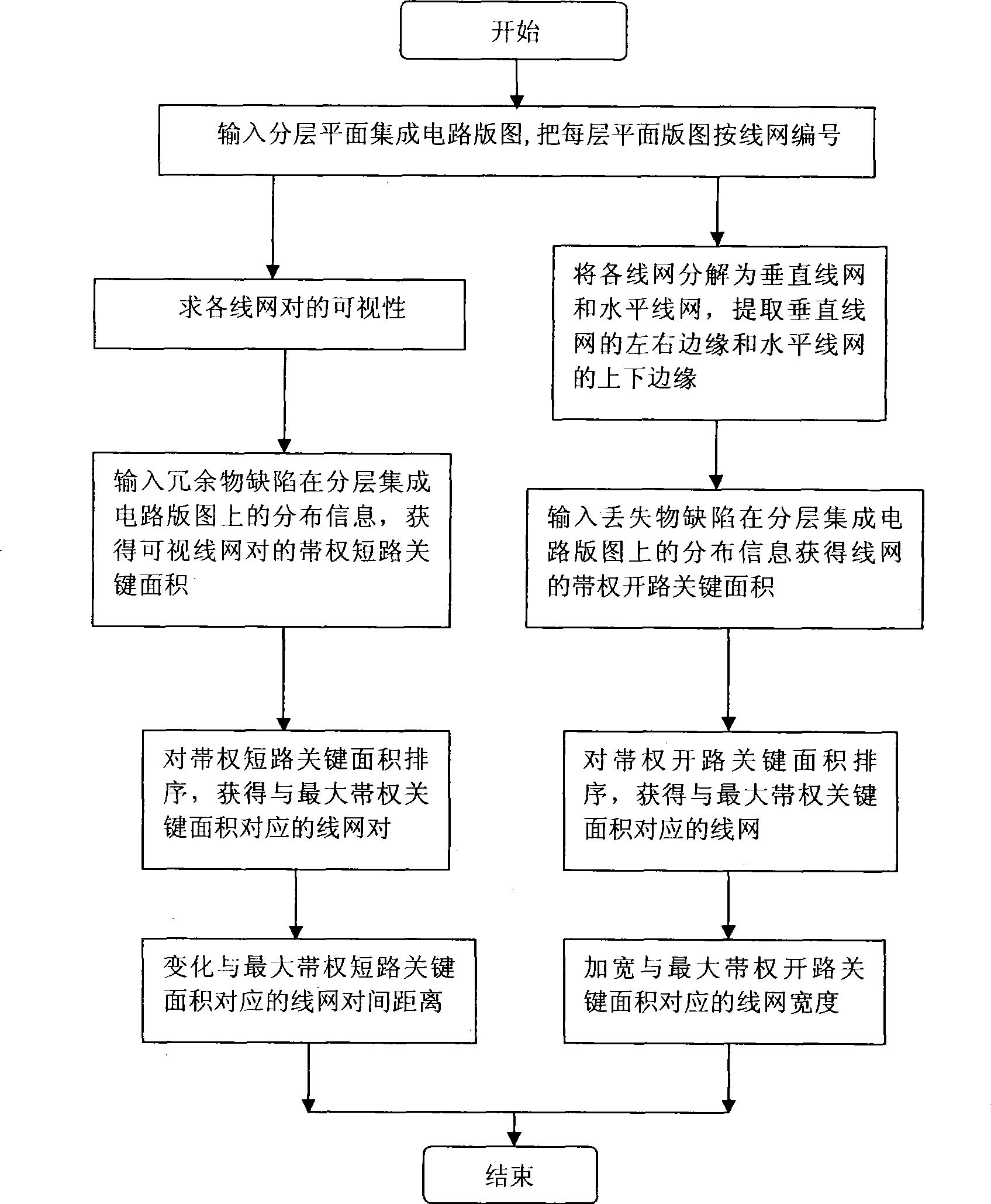
[0067] refer to figure 1 The layout optimization method implemented in the present invention is to characterize the defect parameters on the basis of the collected defect characteristic parameters related to the integrated circuit technology of each layer, and then optimize the plane layout of different process layers according to the plane layout of the input integrated circuit chip . Defect characteristic parameters related to each layer process generally include defect shape, defect particle size distribution, and defect spatial distribution characteristics. In the embodiment of the present invention, the layout of the integrated circuit can be intuitively optimized according to the analyzed defect data, and the specific process is as follows:

[0068] In the first step, the planar layout of each layer of the integrated circuit to be estimated is numbered according to the net.

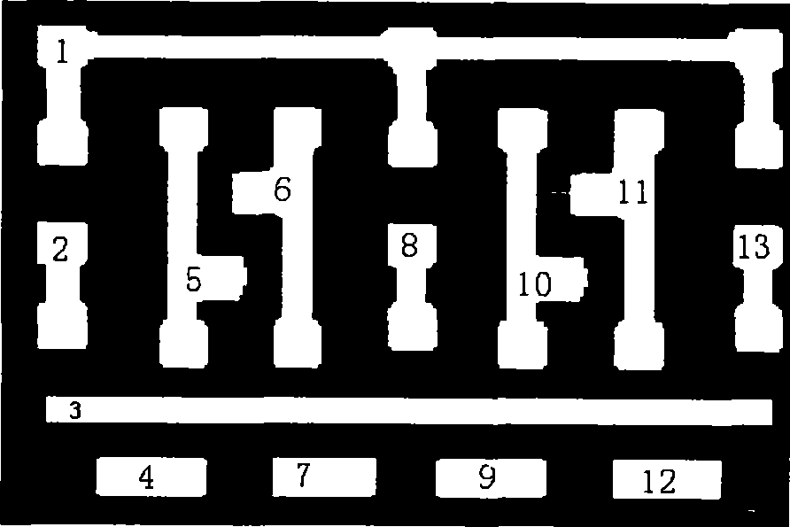
[0069] First, the layout is decoded to form a two-color multi-layer planar layout; then, each ...


PUM


Abstract

The invention discloses a method for utilizing mathematical morphology to optimize integrated circuit layout, aiming at solving the problems of low precision and non-intuitionism of the prior optimizing method. Different layout optimizing methods are adopted by the invention for defects of different types. In the specific process, the plane layout of each layer of an integrated circuit to be estimated is numbered according to wire mesh; for redundant material defects, cum right key areas of short circuits are extracted; the cum right key areas of the short circuits are sorted according to wire mesh pairs; according to the sorting result, the layout is optimized for the first time; for missing material defects, cum right key areas of open circuits are extracted; the cum right key areas of the open circuits are sorted according to the wire mesh and the layout is optimized for the second time according to the sorting result. The method for utilizing mathematical morphology to optimize integrated circuit layout has the advantages of high optimizing precision, simplicity and easy operation and can be used for optimizing the integrated circuit layout in the microelectronic field to further improve the yield of integrated circuits.

Description

technical field [0001] The invention relates to the technical field of microelectronics, in particular to an integrated circuit layout optimization method, which can be used to improve the manufacturing yield of integrated circuit chips. Background technique [0002] As the large-scale integrated circuit VLSI technology enters the 90nm and 65nm technology node process, the yield loss caused by random defects is becoming more and more serious. Since it is difficult to overcome the yield loss caused by random defects in the standard manufacturing environment of 90nm and below, the yield design that relies on design to reduce yield loss has become an effective method to improve yield. [0003] When performing yield design, it is required to consider the defect information that causes random yield loss in the design stage, especially the layout design stage, and improve the design based on this information to reduce the yield loss. The key parameters that usually link yield los...

Claims


Application Information

Patent Timeline
IPC IPC(8): G06F17/50
Inventor 王俊平郝跃方敏
Owner XIDIAN UNIV
Why Eureka
Try Eureka