Process for manufacturing split chip
A kind of chip and partial ground technology, applied in semiconductor/solid-state device manufacturing, semiconductor devices, electrical components, etc., can solve problems such as surface difficulties, chip damage, chip jumping or contact, etc., and achieve the effect of easy picking and dividing chips
Inactive Publication Date: 2010-12-01
3M INNOVATIVE PROPERTIES CO
View PDF8 Cites 0 Cited by
- Summary
- Abstract
- Description
- Claims
- Application Information
AI Technical Summary
Problems solved by technology
Method used
View moreImage
Smart ImageViewing Examples

Examples
example 1
Login to View More PUM
 Abstract
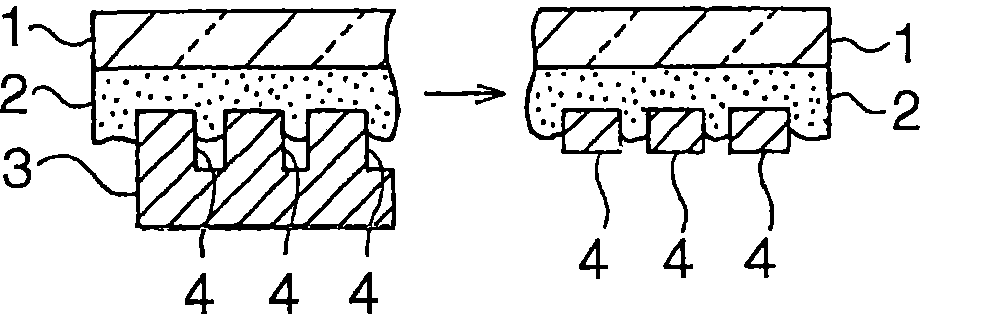
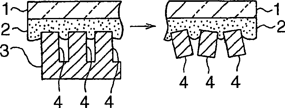
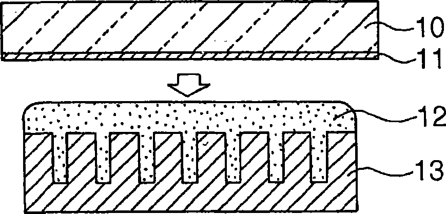
To provide a method of producing segmented chips preventing the chips from being damaged by the chip jumping or by the contact of the neighboring chips while the back surfaces thereof are being ground. A method of producing segmented chips by grinding the back surface of a material to be ground which includes a plurality of chips segmented into individual chips by at least partly cutting the chips in the direction of thickness thereof along the boundaries of the chips, wherein the gaps among the individual chips are filled with a liquid adhesive, the material to be ground is laminated on a rigid support material in a manner that the back surface thereof is exposed, and the adhesive is cured or solidified to form a laminate of the material to be ground having the plurality of chips, the adhesive solid material and the rigid support material arranged in this order; the laminate is ground from the back surface side of the material to be ground, the rigid support member is removed from the laminate, a flexible adhesive sheet is adhered onto the adhesive solid material, and the individual chips are picked up and recovered.
Description
Method for preparing split chips technical field The present invention relates to methods for preparing segmented chips. Background technique In recent years, semiconductor chips of reduced thickness have tended to be produced, and reduction in thickness to 50 to 100 μm or less has been expected. To reduce the thickness of semiconductor chips, it is generally accepted practice to grind the back surface of a wafer having multiple chips, followed by dicing to form thin individual chips. The following techniques are known as methods of grinding the back surface. First, a laminate structure comprising wafer / adhesive layer / support material is processed by adhering the circuit surface of the wafer to the support material with an adhesive layer. The wafer side of the stack is ground to grind the back surface. After the back surface is ground, the support material and adhesive layer are removed, followed by dicing to separate the wafer into individual chips. As a method of ...
Claims
Login to View More Application Information
Patent Timeline
 Patent Type & Authority Patents(China)
IPC IPC(8): H01L21/301H01L21/78H01L21/304
CPCH01L21/6836H01L21/6835H01L21/67092H01L2221/68336H01L21/3043H01L2221/68322H01L2221/68327H01L21/67132H01L2221/68359H01L21/78H01L21/30H01L21/304
Inventor 秋山良太齐藤一太
Owner 3M INNOVATIVE PROPERTIES CO
Features
- R&D
- Intellectual Property
- Life Sciences
- Materials
- Tech Scout
- Unparalleled Data Quality
- Higher Quality Content
- 60% Fewer Hallucinations
Learn More Browse by: Latest US Patents, China's latest patents, Technical Efficacy Thesaurus, Application Domain, Technology Topic, Popular Technical Reports.
© 2025 PatSnap. All rights reserved.Legal|Privacy policy|Modern Slavery Act Transparency Statement|Sitemap|About US| Contact US: help@patsnap.com