Bonding pad structure and semiconductor device including the bonding pad structure

A semiconductor and device technology, applied in the field of semiconductor devices and manufacturing semiconductor devices, can solve problems such as device degradation and device failure

Inactive Publication Date: 2009-07-29
SAMSUNG ELECTRONICS CO LTD
View PDF1 Cites 5 Cited by
  • Summary
  • Abstract
  • Description
  • Claims
  • Application Information

AI Technical Summary

Problems solved by technology

Oxidation of the copper lower metal layer 12 degrades the device or causes the device to fail

Method used


Image

  • Bonding pad structure and semiconductor device including the bonding pad structure
  • Bonding pad structure and semiconductor device including the bonding pad structure
  • Bonding pad structure and semiconductor device including the bonding pad structure

Examples


Embodiment Construction

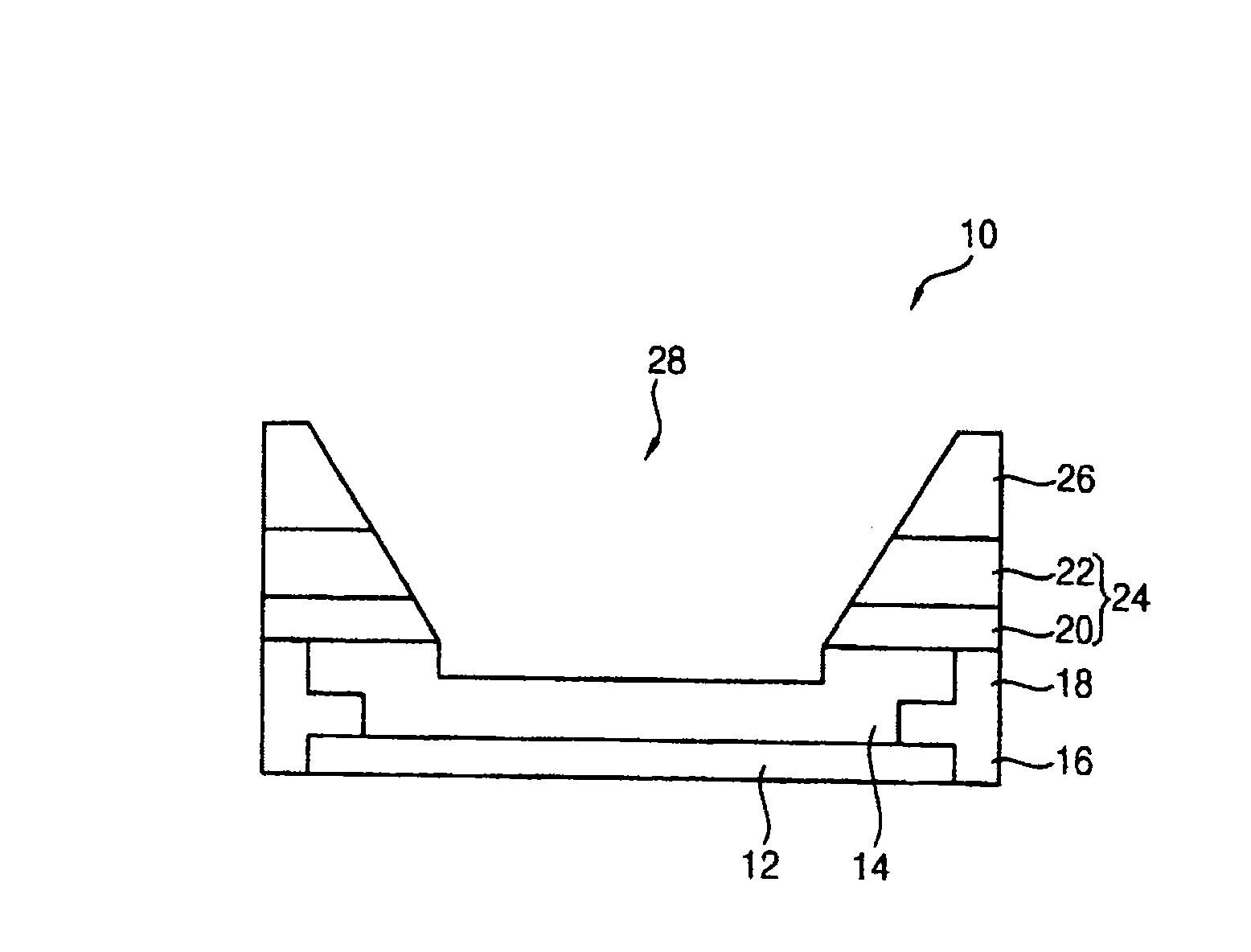
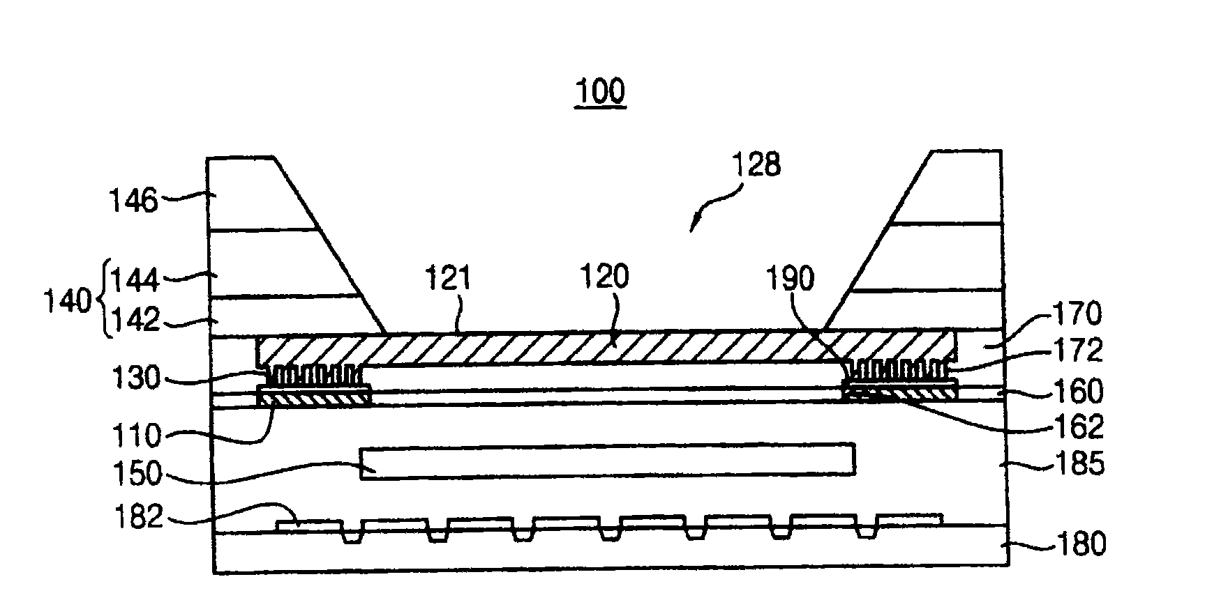
[0056] figure 2 is a schematic cross-sectional view of a pad structure 100 for a semiconductor device according to an embodiment of the present invention. The pad structure 100 is formed on a semiconductor substrate 180 . Various devices 182 are formed in substrate 180 . An inter-layer dielectric (ILD) layer 185 is formed on the device 182 . An optional probing protection layer 150 (which may be formed from an insulating or conductive material) is optionally formed in the ILD layer 185 . A first metal layer or lower pad layer 110 in a first interlayer metal dielectric (IMD) layer 160 is formed on the ILD layer 185 . The first IMD layer 160 includes a trench region 162 in which the metal conductive portion of the lower pad layer 110 is formed. The first metal layer or the lower pad layer 110 may be formed of, for example, copper or aluminum. A barrier metal layer 190 may be formed on the lower pad layer 110 to prevent migration of the material of the lower pad layer 110 d...


PUM


Abstract

A bonding pad structure for a semiconductor device includes a first lower metal layer beneath a second upper metal layer in a bonding region of the device. The lower metal layer is formed such that the metal of the lower metal layer is absent from the bonding region. As a result, if damage occurs to the structure during procedures such as probing or bonding at the bonding region, the lower metal is not exposed to the environment. Oxidation of the lower metal layer by exposure to the environment is prevented, thus improving reliability of the device.

Description

technical field [0001] The present invention relates to semiconductor devices and methods of manufacturing semiconductor devices. In particular, the present invention relates to a bonding pad structure for a semiconductor device, a semiconductor device including the bonding pad structure, and a method of manufacturing the bonding pad structure and the semiconductor device including the bonding pad structure. Background technique [0002] Semiconductor devices typically include bonding pads formed from conductive layers, such as metal layers. Bonding pads are commonly used to measure the electrical characteristics of semiconductor devices. During testing, the probes are in contact with the semiconductor device at the bonding pads. The pads are also used to make electrical contact with bonding wires or bumps when the semiconductor device is mounted in a package. [0003] figure 1 is a schematic cross-sectional view of a conventional pad structure 10 in a semiconductor devi...

Claims


Application Information

Patent Timeline
Patent Type & Authority Applications(China)
IPC IPC(8): H01L23/498H01L21/60
CPCH01L2224/05093H01L2924/01032H01L2924/01023B32B15/018H01L2924/01046H01L2924/0105H01L2924/01082H01L2924/01004B32B15/017H01L2924/15311H01L2924/01029H01L2224/05567H01L2924/01022H01L2924/01028H01L2224/05181H01L2224/48091H01L2924/01087B32B15/01H01L2224/05556H01L2924/014H01L2924/01013H01L2224/05571H01L24/03H01L2924/04941H01L2924/05042H01L2924/04953H01L2924/01079H01L24/05H01L2224/48227H01L2224/04042H01L2924/01033H01L2924/01006H01L2924/01074H01L2924/01078H01L2924/01014H01L2924/01073H01L2924/3025H01L2224/02166H01L2224/05553H01L2924/00014H01L2924/0002Y10T428/12528Y10T428/12701Y10T428/12736Y10T428/12882Y10T428/12896Y10T428/12931Y10T428/31678H01L2224/05552H01L23/48
Inventor 洪琮沅崔吉铉黄烘奎李钟鸣郭旻根成金重
Owner SAMSUNG ELECTRONICS CO LTD
Why Eureka
Try Eureka