
Interface control method for mainboard and memory slots thereof

A technology of memory slot and control method, which can be used in instruments, electrical digital data processing, etc., and can solve problems such as hardware cost increase

Active Publication Date: 2010-02-17
ASUSTEK COMPUTER INC
View PDF0 Cites 0 Cited by
  • Summary
  • Abstract
  • Description
  • Claims
  • Application Information

AI Technical Summary

Problems solved by technology

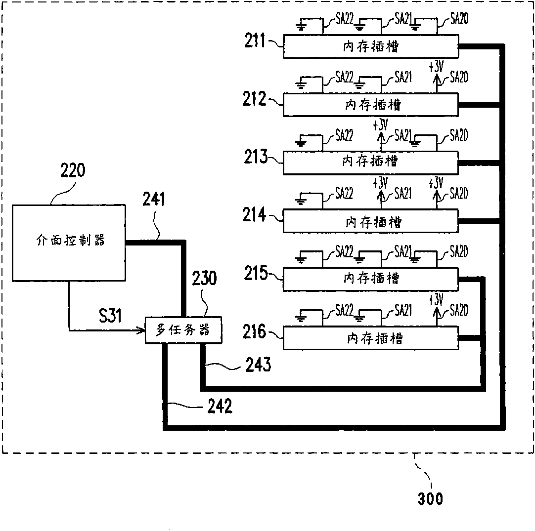
At this time, it is known that the hardware cost of the motherboard 300 will also increase with the increase of the multi-taskers

Method used


Image

  • Interface control method for mainboard and memory slots thereof
  • Interface control method for mainboard and memory slots thereof
  • Interface control method for mainboard and memory slots thereof

Examples


Embodiment Construction

[0024] Figure 4 Shown is a schematic diagram of some components of a motherboard according to an embodiment of the present invention. The mainboard 400 includes a plurality of slot groups 410_1 to 410_N, an interface controller 420 and a bus 430 . The socket groups 410_1 to 410_N each include a first memory socket 411 and a second memory socket 412 . The first memory slot 411 and the second memory slot 412 each have a plurality of connection ends. For the convenience of description, the following description will be given by taking an example that each of the first memory slot 411 and the second memory slot 412 has three connection terminals.

[0025] In this embodiment, the first memory slot 411 has three connecting ends TM1(1)-TM1(3), and the second memory slot 412 has three connecting ends TM2(1)-TM2(3). In other words, the slot groups 410_1 to 410_N correspond to the six connection terminals TM1(1) to TM1(3) and TM2(1) to TM2(3) respectively. In the overall configurat...


PUM


Abstract

The invention provides an interface control method for a mainboard and memory slots thereof. The mainboard comprises a plurality of slot groups, a bus and an interface controller, wherein each of theslot groups comprises a first memory slot and a second memory slot which are connected to the bus respectively; the first memory slot and the second memory slot form two different access addresses; the interface controller sends a plurality of pin control signals to corresponding slot groups to make the two access addresses of the first memory slot and the second memory slot of a using slot groupamong the slot groups different from two access addresses of the first memory slot and the second memory slot of the other slot groups; and the interface controller performs an access action on the using slot group through the bus.

Description

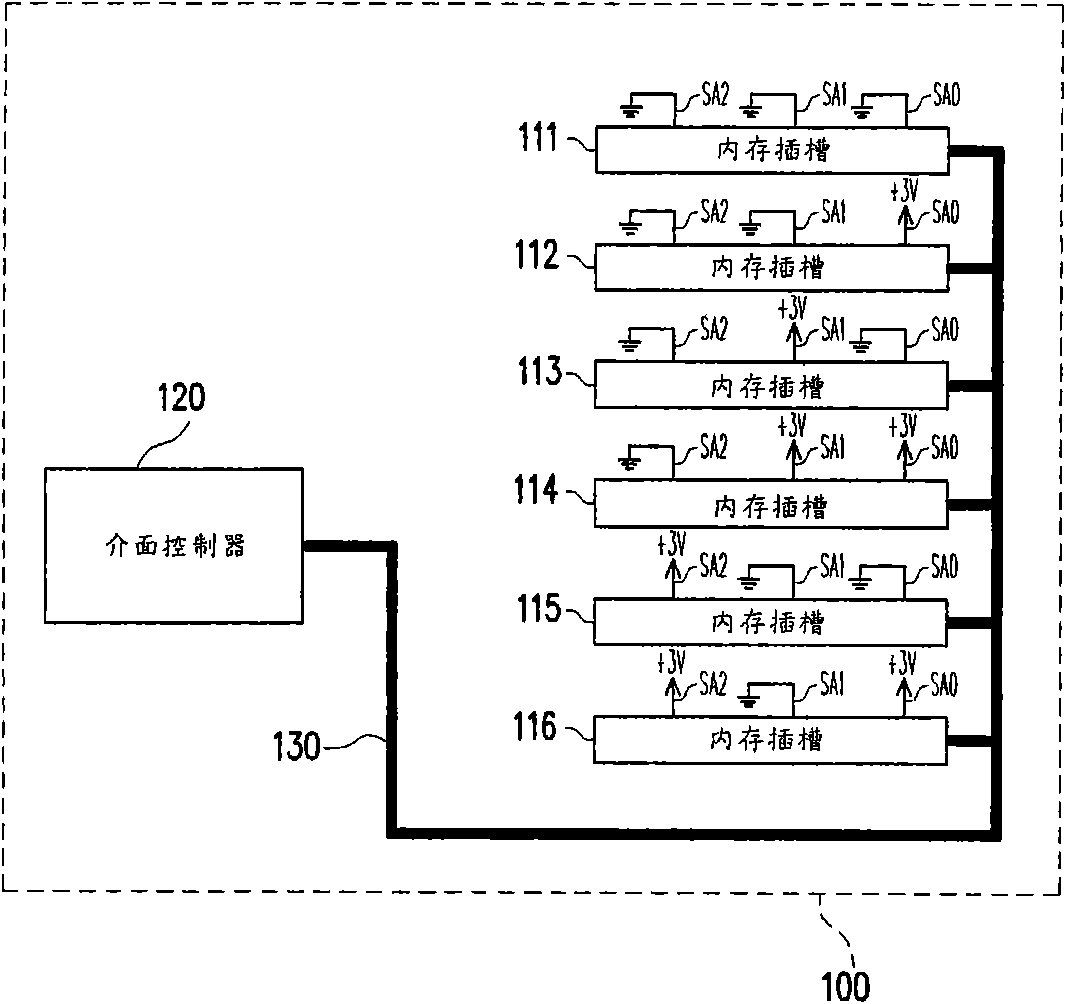
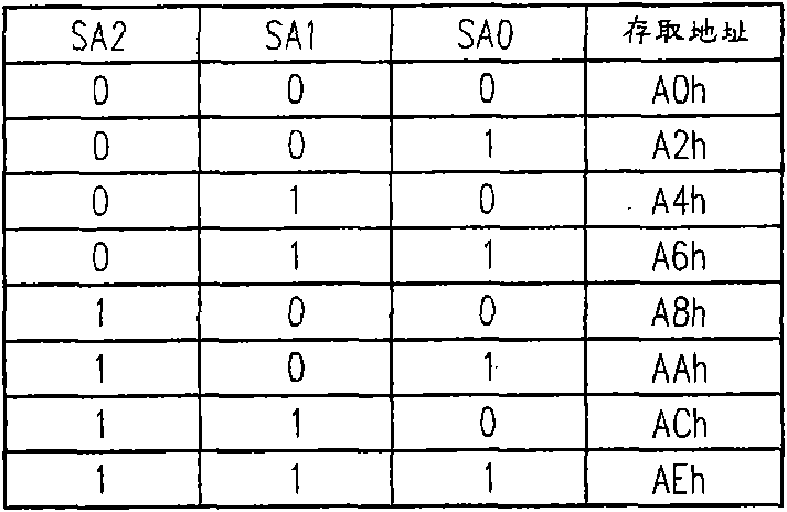
technical field [0001] The present invention relates to a mainboard, and more particularly, to a mainboard that can effectively utilize memory modules. Background technique [0002] A personal computer system is mainly composed of a motherboard, interface cards and peripheral devices, among which the motherboard can be said to be the heart of the computer system. On the motherboard, in addition to a central processing unit (central processing unit), a control chip set (chip set) and slots for installing interface cards, there are also several memory slots for installing memory modules. A memory module is composed of several memory components, and according to user requirements, different numbers of memory modules can be installed on the motherboard. [0003] figure 1 It is a schematic diagram of some components of a known motherboard. refer to figure 1 It is known that the motherboard 100 includes memory slots 111 - 116 , an interface controller 120 and a system manageme...

Claims


Application Information

Patent Timeline
Patent Type & Authority Applications(China)
IPC IPC(8): G06F13/16
Inventor 李明任吴东璋
Owner ASUSTEK COMPUTER INC
Learn More