Method of determining graphic outer contour for optical proximity correction

A technology of optical proximity correction and outer contour, which is applied in photomechanical processing of originals, optics, and pattern surfaces for opto-mechanical processing.

Inactive Publication Date: 2010-06-23
SEMICON MFG INT (SHANGHAI) CORP
View PDF1 Cites 7 Cited by
  • Summary
  • Abstract
  • Description
  • Claims
  • Application Information

AI Technical Summary

Problems solved by technology

Therefore, there is a demand in the industry to basically maintain the calculation accuracy of the outer contour of the circuit layout graph 10, and reduce the number of test points, thereby reducing the amount of calculation.

Method used


Image

  • Method of determining graphic outer contour for optical proximity correction
  • Method of determining graphic outer contour for optical proximity correction
  • Method of determining graphic outer contour for optical proximity correction

Examples


Embodiment Construction

[0025] The inventors of the present invention found that when performing optical proximity correction to determine the outline of the figure, there is redundancy in the test points used to determine the outline of the figure, such redundancy greatly increases the amount of calculation when performing optical proximity correction, and cannot adapt to Optical proximity correction for increasingly dense circuit layouts.

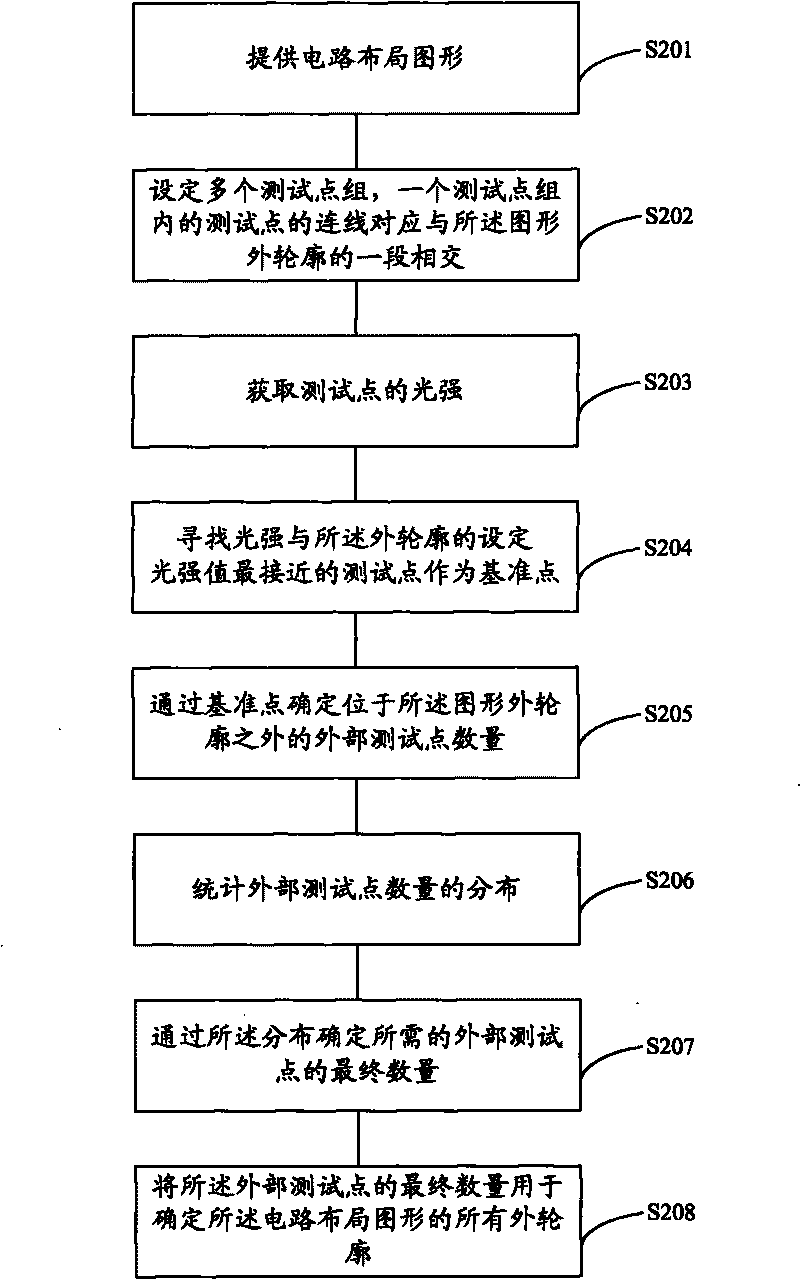
[0026] In order to reduce the redundancy of test points, according to an embodiment of the present invention, a method for determining the outer contour of a graph for optical proximity correction is provided, such as figure 2 shown, including steps:

[0027] S201, providing circuit layout graphics;

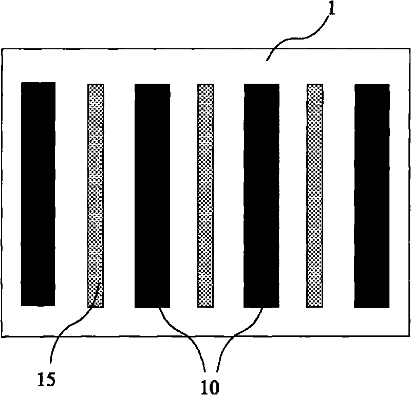
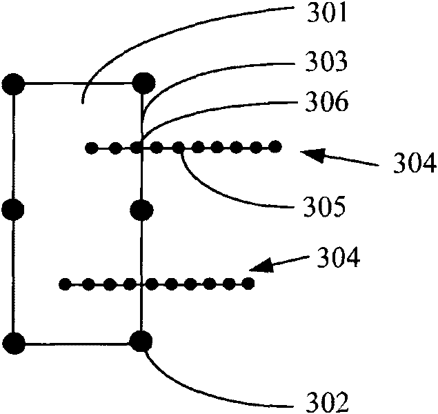
[0028] S202, setting a plurality of test point groups, the connection line of the test points in each test point group correspondingly intersects with a section of the outer contour of the graph;

[0029] S203, acquiring the light intensity of the test point;

...


PUM


Abstract

The invention provides a method of determining graphic outer contour for optical proximity correction (OPC), comprising the steps of providing a circuit layout graphic; setting a plurality of test point groups, wherein the connecting lines of the test points in each test point group are correspondingly crossed with one section of the graphic outer contour; obtaining light intensities of the test points; searching a test point, the light intensity of which is proximal to a preset light intensity of the outer contour, as a reference point; determining the number of outer test points out of the graphic outer contour by the reference point; counting the distribution of the number of the outer test points; determining the final number of the required outer test points by the distribution; and determining all outer contours of the circuit layout graphic by the final number of the outer test points. Compared with the prior art, the invention can reduce the number of the outer test points and the amount of calculation of the OPC on the premise of basically keeping the calculation precision.

Description

technical field [0001] The invention relates to the manufacturing field of semiconductor devices, in particular to a method for determining the outer contour of a figure for optical proximity correction. Background technique [0002] With the rapid development of semiconductor manufacturing technology, in order to achieve faster computing speed, larger data storage capacity and more functions of semiconductor devices, semiconductor chips are developing towards higher integration. The higher the integration degree of the semiconductor chip, the smaller the critical dimension (CD, Critical Dimension) of the semiconductor device. [0003] However, due to the impact of the resolution limit of the optical exposure tool (optical exposure tool), it is easy to produce the optical proximity effect ( OPE (optical proximity effect), such as right-angled comer rounded, line end shortened, and line width increase / decrease, are common optical proximity The defect caused by the transfer ...

Claims


Application Information

Patent Timeline
Patent Type & Authority Applications(China)
IPC IPC(8): G03F1/14G03F1/00G03F1/36G03F1/70
Inventor 王伟斌张飞
Owner SEMICON MFG INT (SHANGHAI) CORP
Why Eureka
Try Eureka