
Display device and driving method of display panel thereof

A technology for display devices and display panels, applied in static indicators, instruments, etc., to solve problems such as short pixel charging time

Active Publication Date: 2014-02-12
AU OPTRONICS CORP
View PDF6 Cites 0 Cited by
  • Summary
  • Abstract
  • Description
  • Claims
  • Application Information

AI Technical Summary

Problems solved by technology

Therefore, if the RC delay time of the signal (that is, the delay time of the resistor and capacitor) is considered, such a short pixel charging time seems to be insufficient

Method used


Image

  • Display device and driving method of display panel thereof
  • Display device and driving method of display panel thereof
  • Display device and driving method of display panel thereof

Examples


no. 1 example

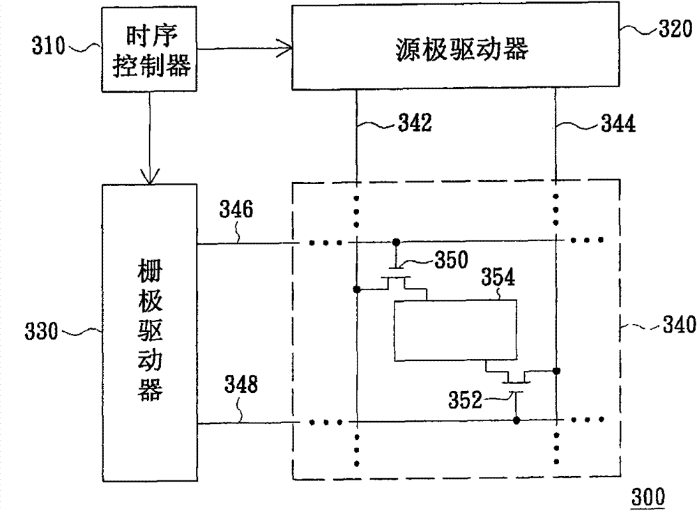
[0039] image 3 is a schematic diagram of a display device according to an embodiment of the present invention. Please refer to image 3, the display device 300 includes a timing controller 310 , a source driver 320 , a gate driver 330 and a display panel 340 . The timing controller 310 is used to control the operation of the source driver 320 and the gate driver 330 so that the source driver 320 and the gate driver 330 can control the display panel 340 to display desired images.

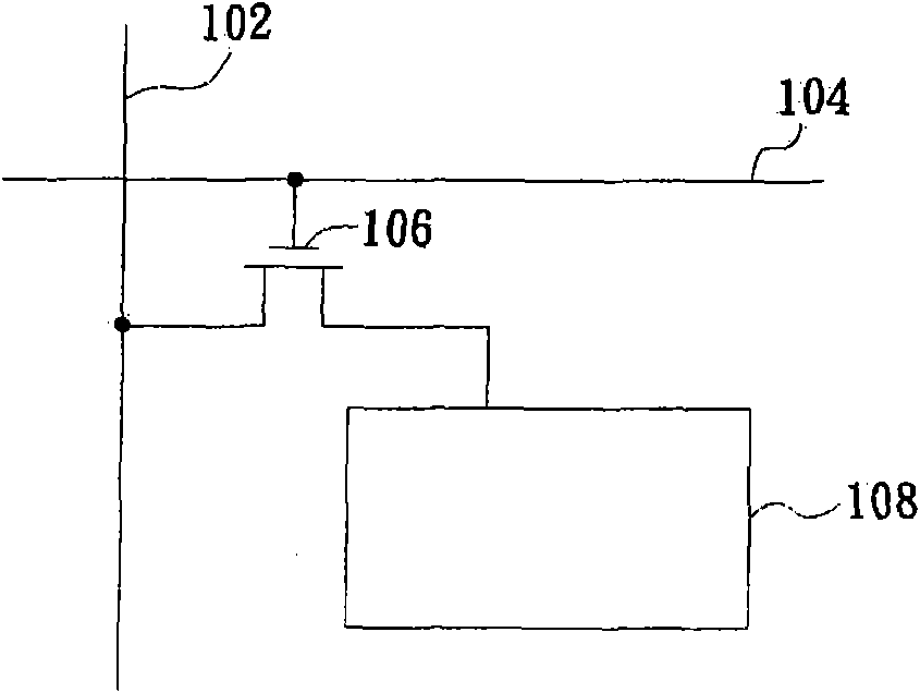
[0040] The display panel 340 adopts a special pixel driving structure, which includes source lines 342 and 344 , gate lines 346 and 348 , and transistors 350 and 352 for driving a pixel 354 . As shown in the figure, the pixel 354 is electrically coupled to two different source lines and two different gate lines through two transistors. In addition, each source line mentioned above is electrically coupled to the source driver 320 , and each gate line is electrically coupled to the gate driver 330 ...

no. 2 example

[0049] Image 6 is a schematic diagram of a display device according to another embodiment of the present invention. Please refer to Image 6 , the display device 600 includes a timing controller 610, a source driver composed of source drive units 620-1 and 620-2, and a gate driver composed of gate drive units 630-1 and 630-2. In addition, a display panel 640 is also included. The timing controller 610 is used to control the operation of the source driver units 620-1 and 620-2, and to control the operation of the gate driver units 630-1 and 630-2, so that the two source drivers and the two The gate driver is used to control the display panel 640 to display desired images.

[0050] The pixel structure of the display panel 640 is the same as the pixel structure of the display panel 340 in the first embodiment, but the coupling manners of the source lines and the gate lines are different. by Image 6 For example, the source lines 642 and 644 are electrically coupled to the s...


PUM


Abstract

The invention relates to a display device and a driving method of a display panel thereof. The display device comprises a display panel and a gate driver, wherein the display panel also comprises two gate lines, two source electrode lines, a pixel and two transistors. The pixel is respectively and electrically coupled with the two gate lines after penetrating through the two transistors and also respectively and electrically coupled with the two source electrode lines after penetrating through the two transistors. The gate driver is used for providing a first impulse to one of the gate lines according to preset frequency as well as providing a second impulse to the other gate line according to the preset frequency. The enabling period of the second impulse is behind that of the first impulse; the distance between a rising edge of the second impulse and a rising edge of the first impulse is preset time difference, and the preset time difference is larger than the time span of the enabling period of the first impulse.

Description

technical field [0001] The present invention relates to the field of display technology, and in particular to a display device and a driving method for a display panel thereof. Background technique [0002] figure 1 A pixel structure of an existing display panel is shown. Please refer to figure 1 , this pixel structure is mainly composed of source lines 102 , gate lines 104 , transistors 106 and pixels 108 . As shown in the figure, the gate of the transistor 106 is electrically coupled to the gate line 104, and one source / drain of the transistor 106 is electrically coupled to the source line 102, and the other source / drain of the transistor 106 is electrically coupled to the source line 102. Sexually coupled to pixel 108. [0003] figure 2 It is an explanatory diagram of the driving method of the above-mentioned display panel. exist figure 2 Among them, the symbol SG represents the signal transmitted to the gate line 104 , the symbol 202 refers to the pulse, the sym...

Claims


Application Information

Patent Timeline
IPC IPC(8): G09G3/20
Inventor 陈政鸿林宗正张弘儒
Owner AU OPTRONICS CORP
Learn More