
Image display device

An image display device and technology for display, applied in lighting devices, static indicators, optics, etc., can solve the problems of inability to expand the size of the area, large flickering phenomenon, etc., and achieve the effect of preventing brightness reduction and flickering phenomenon

Inactive Publication Date: 2010-07-21
SHARP KK
View PDF3 Cites 7 Cited by
  • Summary
  • Abstract
  • Description
  • Claims
  • Application Information

AI Technical Summary

Problems solved by technology

The Max method has the advantage of being able to display images with correct brightness, but has the following problems: that is, the flickering phenomenon when displaying moving images is large, and the area size cannot be enlarged due to the large flickering phenomenon

Method used


Image

  • Image display device
  • Image display device
  • Image display device

Examples


Embodiment approach 1

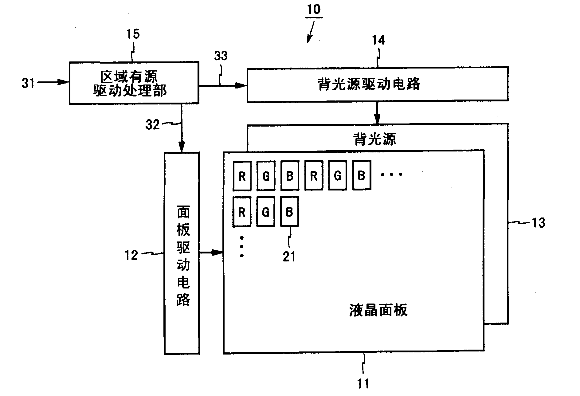
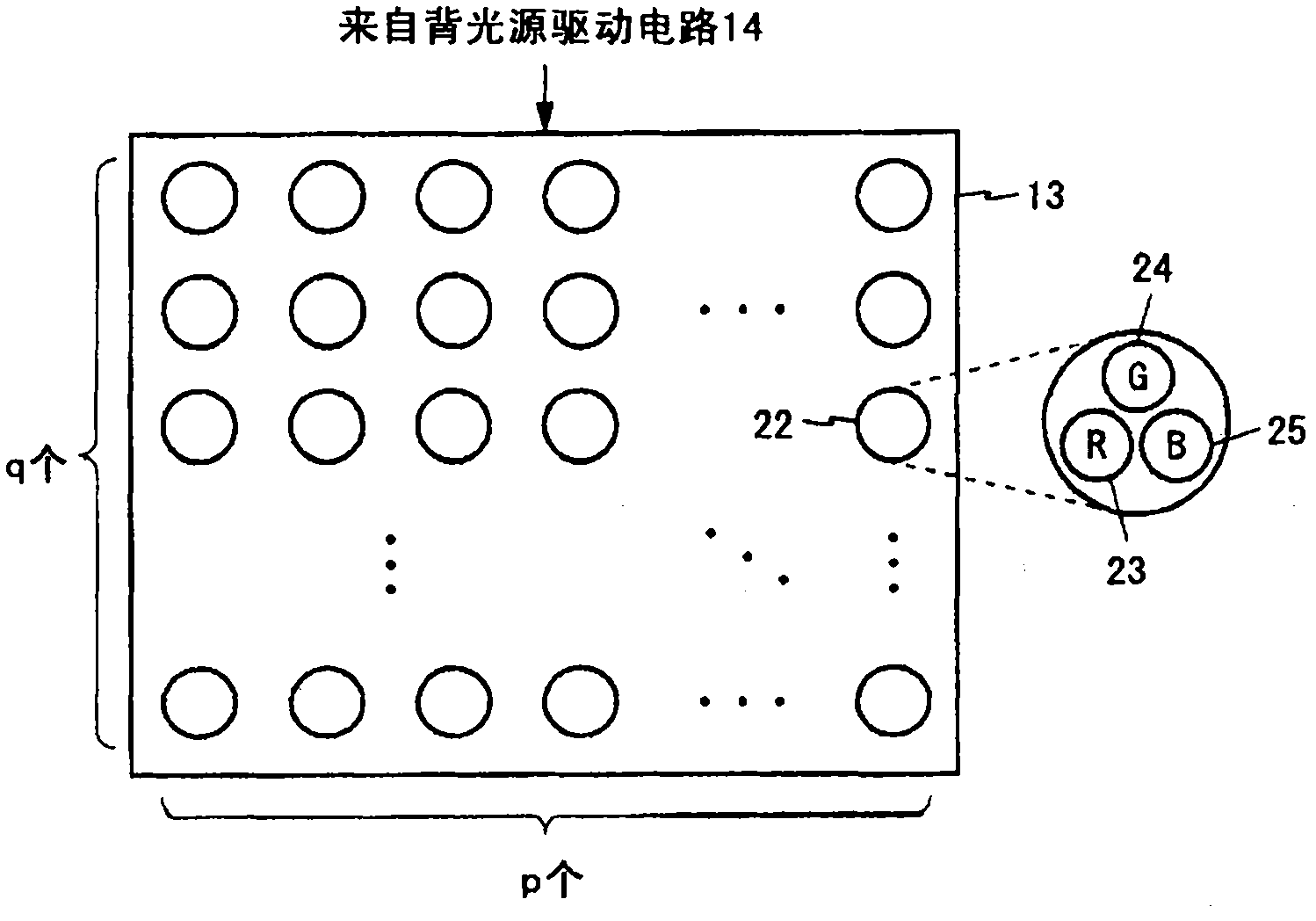
[0072] figure 1 It is a block diagram showing the configuration of the liquid crystal display device according to Embodiment 1 of the present invention. figure 1 The illustrated liquid crystal display device 10 includes: a liquid crystal panel 11 , a panel driving circuit 12 , a backlight 13 , a backlight driving circuit 14 , and an area active driving processing unit 15 . The liquid crystal display device 10 divides the screen into a plurality of regions and performs region active driving. The region active driving is to control the brightness of the light source of the backlight based on the input image in the region and drive the liquid crystal panel 11 . Hereinafter, m and n are integers of 2 or more, p and q are integers of 1 or more, and at least one of p and q is an integer of 2 or more.

[0073] An input image 31 including an R image, a G image, and a B image is input to the liquid crystal display device 10 . The R image, the G image, and the B image all include th...

Embodiment approach 2

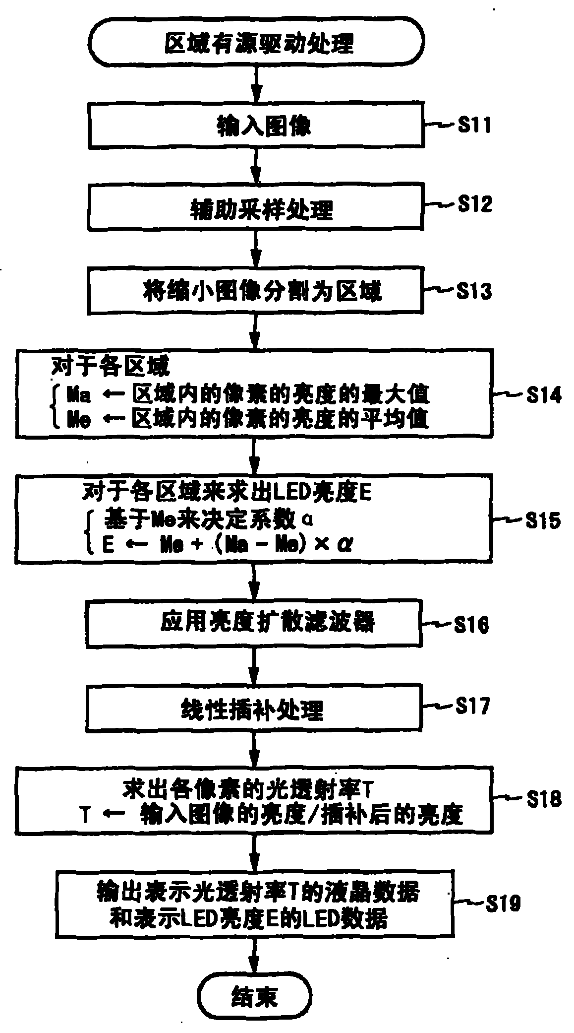
[0110] The liquid crystal display device according to the second embodiment of the present invention has the same structure as the liquid crystal display device 10 according to the first embodiment (see figure 1 ). In the liquid crystal display device according to Embodiment 1, the image 3 In step S15 shown, the coefficient α is determined based on the average value Me of the luminances of the pixels in the area. However, sometimes the coefficient α is smaller than 1, and the coefficient α does not change during display of a still image. Therefore, in the liquid crystal display device according to Embodiment 1, a decrease in luminance during still image display may become a problem.

[0111] Therefore, the liquid crystal display device according to the present embodiment performs a process of bringing the luminance of the LED closer to the luminance of the Max method when the change in the luminance of the pixels in the area is small. Specifically, when the area active dr...


PUM


Abstract

An area active drive processing unit (15) obtains liquid crystal data (32) used for driving a liquid crystal panel (11) and LED data (33) used for driving backlight (13) from an input image (31). In order to obtain the LED data (33), the input image (31) is divided into areas, a maximum value Ma and a mean value Me of luminances of pixels in each area are obtained, and a weighted mean of the maximum value Ma and the mean value Me is obtained, thereby obtaining the luminance of an LED (23)-(25) corresponding to each area. A coefficient a used for obtaining the weighted mean changes depending on the mean value Me. As the mean value Me increases, the LED luminance increases from the mean value Me at an accelerated rate and approaches the maximum value Ma. As a result, flicker and lowering of luminance in an image display device controlling backlight are prevented.

Description

technical field [0001] The present invention relates to an image display device, and more particularly to an image display device having a function of controlling the brightness of a backlight (backlight dimming function). Background technique [0002] In an image display device including a backlight such as a liquid crystal display device, by controlling the brightness of the backlight based on an input image, the power consumption of the backlight can be suppressed and the image quality of the displayed image can be improved. In particular, by dividing the screen into a plurality of areas and controlling the luminance of the light source of the backlight corresponding to the area based on the input image in the area, it is possible to further achieve lower power consumption and higher image quality. Hereinafter, the method of controlling the luminance of the light source of the backlight based on the input image in the area to drive the display panel as described above is ...

Claims


Application Information

Patent Timeline
Patent Type & Authority Applications(China)
IPC IPC(8): G09G3/36G02F1/133G09G3/20G09G3/34F21Y101/02
CPCG09G2320/0247G02F1/133603G09G2360/16G09G3/3426G09G2320/0653G09G2320/0646G09G2320/0261
Inventor 藤原晃史
Owner SHARP KK
Learn More