Display device and display method

a display device and display method technology, applied in the field of display devices, can solve the problems of deterioration of display, unavoidable formation of parasitic capacitance between the gate, flickering of a displayed image, etc., and achieve the effect of suppressing the occurrence of flickering

Inactive Publication Date: 2005-03-15
SHARP KK
View PDF15 Cites 23 Cited by
  • Summary
  • Abstract
  • Description
  • Claims
  • Application Information

AI Technical Summary

Benefits of technology

The present invention is made in light of the aforementioned problems of the prior art, and the object of the present invention is to provide a display device which is capable of sufficiently suppressing occurrence of flickering and the like which ensue to fluctuations of pixel potentials caused by parasitic capacitances, and which is high-definition and high-performance.
According to the foregoing display device, however, the falls of the scanning signal are controlled, and hence it is possible to control the scanning signal so that it does not abruptly fall. This ensures that the level shifts of the pixel potentials caused by the parasitic capacitances are reduced.
Further, wires laid on a transparent insulating substrate made of, for example, glass are not an ideal path but constitute a signal delay path which undergoes signal delay to some extent. Therefore, the foregoing arrangement ensures that irregularities of display caused by the signal delay are cancelled, and moreover, that the level shifts caused to the pixel potentials by the parasitic capacitances are made smaller and uniform. In result, displayed images of high performance can be obtained.

Problems solved by technology

Generally, parasitic capacitances are unavoidably formed between the gate and the drain of the thin film transistor due to the structure.
Such significant level shift occurring to the pixel potential leads to flickering of a displayed image, deterioration of display, and the like.

Method used


Image

  • Display device and display method
  • Display device and display method
  • Display device and display method

Examples


first embodiment

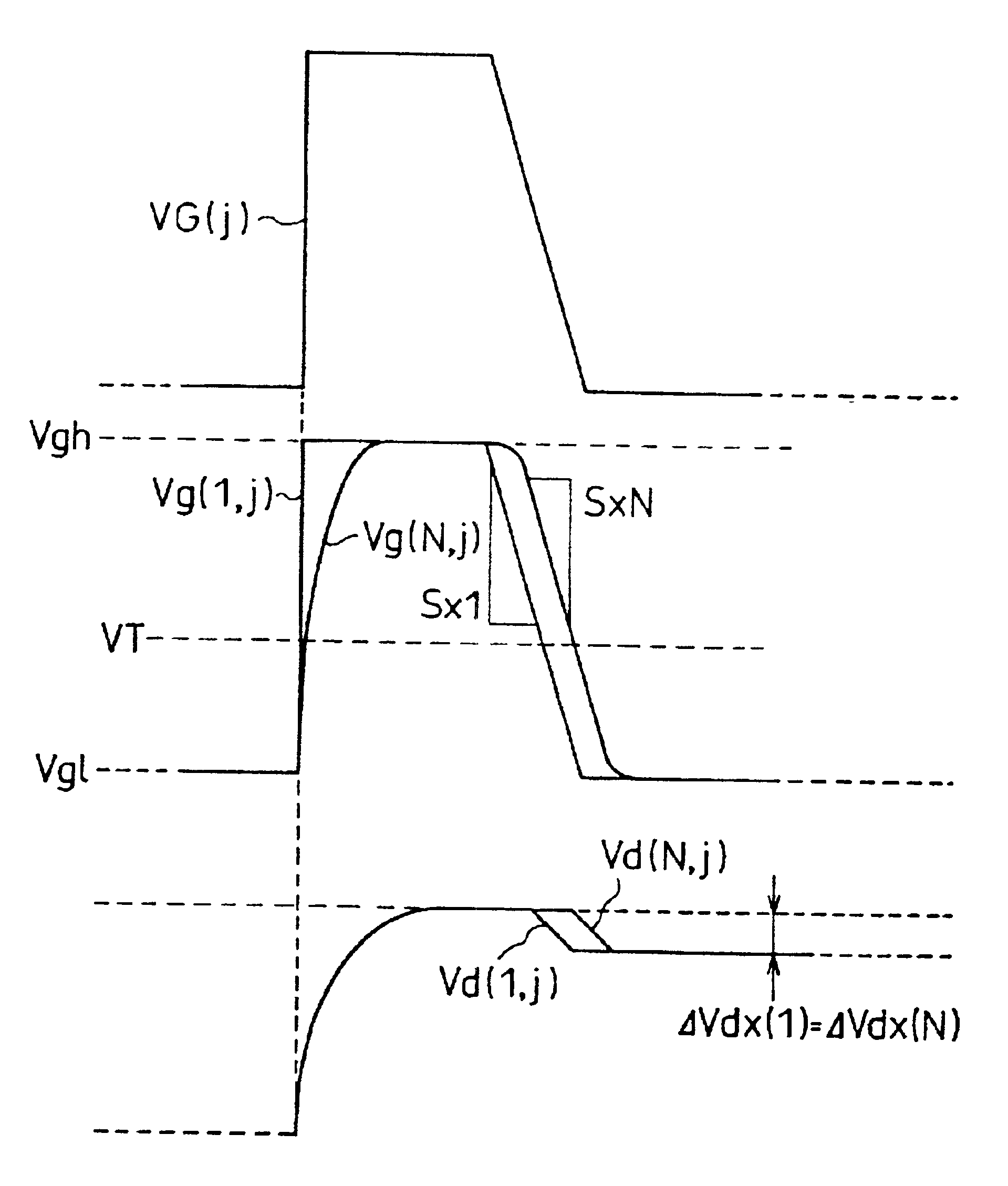
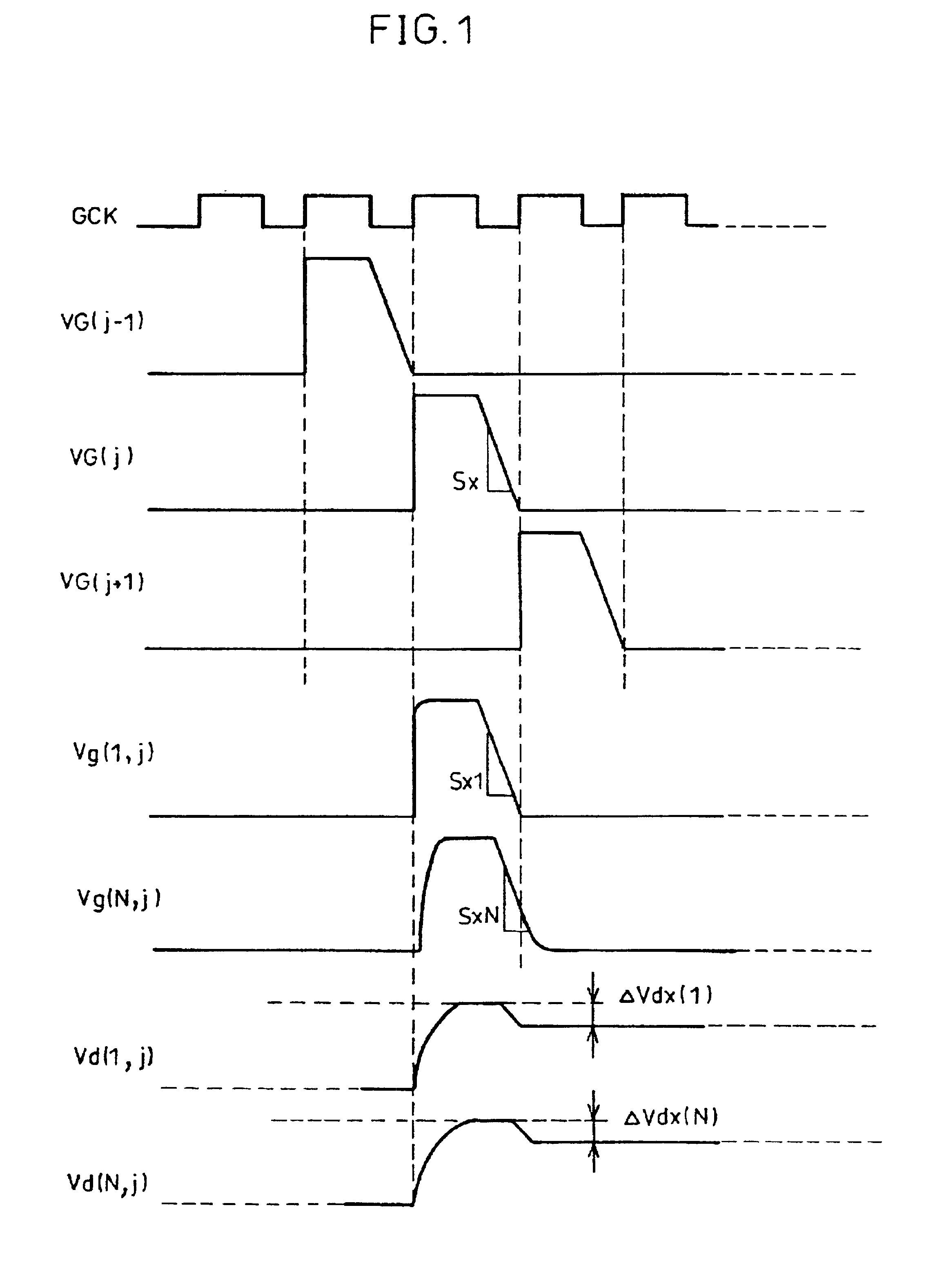
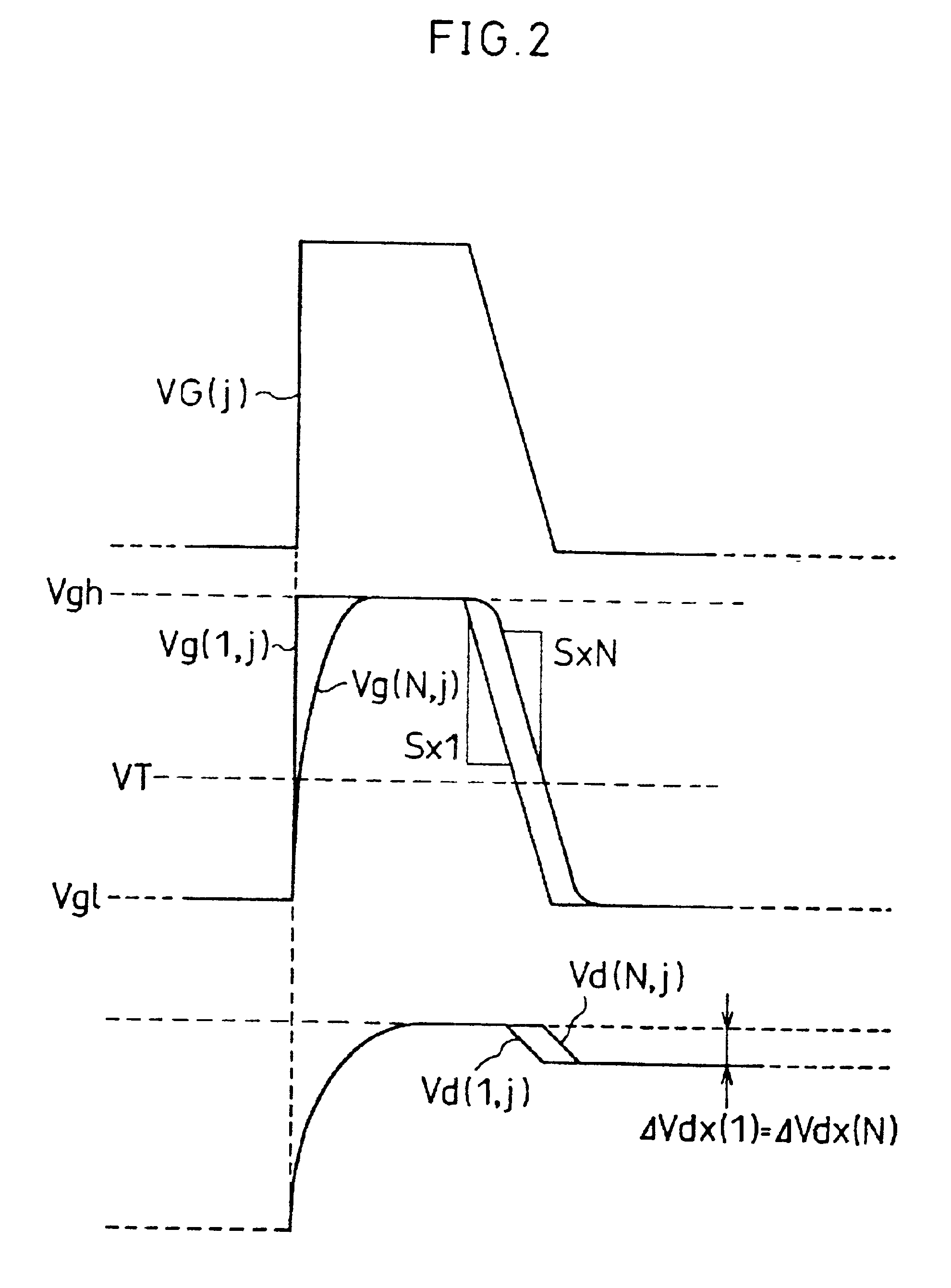
The following description will explain a first embodiment of the present invention while referring to FIGS. 1 and 2. Note that in FIG. 1 GCK represents a clock signal.

FIGS. 1 and 2 show output waveforms VG(j−1), VG(j), and VG(j+1) of a scanning signal line driving circuit in accordance with the present embodiment, a scanning signal line waveform Vg(1, j) in the vicinity of an input-side end of a scanning signal line, a scanning signal line waveform Vg(N, j) in the vicinity of the other end of the scanning signal line, and respective pixel potentials Vd(1, j) and Vd(N, j) in the vicinity of the foregoing ends of the scanning signal line. In the output waveform VG(j) of the scanning signal line driving circuit, the fall from a scanning voltage Vgh to a non-scanning voltage Vgl is a fall at a slope (inclination) indicated by a change rate Sx, which is a change quantity per unit time, as shown in FIG. 1.

The present embodiment has a display system in which data signals are supplied to a ...

second embodiment

The following description will explain a second embodiment of the present invention, while referring to FIG. 3. For conveniences' sake, the members having the same structure (function) as those in FIG. 10 will be designated by the same reference numerals.

In the second embodiment of the present invention, as shown in FIG. 3, as in the case of the conventional scanning signal line driving circuit shown in FIG. 10, the scanning signal line driving circuit is composed of a shift register section 3a composed of M flip-flops (F1, F2, . . . , Fj, . . . , FM) cascaded, and selection switches 3b which are opened / closed in accordance with outputs from the flip-flops, respectively. An input terminal VD1 out of two input terminals of each selection switch 3b is supplied with a gate-on voltage Vgh which is enough to cause the TFT to attain an ON state, while the other input terminal VD2 thereof is supplied with a gate-off voltage Vgl which is enough to cause the TFT to attain an OFF state. A com...

third embodiment

As to the above-described second embodiment, a case where the slew-rate control element SC for controlling the fall speed (slope) of the scanning signal is added to the conventional structure of the scanning signal line driving circuit (gate driver) is explained. In this case, however, it is necessary to additionally provide the slew-rate control element SC in the gate driver, and the conventional common inexpensive gate driver cannot be applied as it is. Therefore it is not economical.

In the third embodiment of the present invention, a conventional inexpensive common gate driver is used. This case will be explained below, with reference to FIGS. 4 and 5.

The conventional gate driver is, as explained above with reference to FIG. 10, arranged as follows: the gate-on voltage Vgh and the gate-off voltage Vgl are supplied thereto, and in response to the clock signal GCK, the gate driver outputs the scanning ON voltage Vgh to the scanning signal lines 105 sequentially, i.e., to one line d...


PUM

PropertyMeasurementUnit
gate-on voltageaaaaaaaaaa
gate-off voltageaaaaaaaaaa
voltageaaaaaaaaaa

Abstract

In the display device and the display method of the present invention, a scanning signal line driving circuit controls falls of a scanning signal line, so as to make level shifts occurring to pixel potentials substantially uniform throughout display plane, the level shifts being caused by parasitic capacitances which parasitically exist in scanning signal lines. Fall waveforms of the scanning signal change at a change rate Sx which is a change quantity per unit time, and by desirably setting the change rate Sx, a change rate Sx1 in the vicinity of an input-side end of the scanning signal line and a change rate SxN in the vicinity of the other end thereof are substantially equal to each other, not being influenced by signal delay transmission characteristic which the scanning signal line possesses, like scanning signal line waveforms Vg(1, j) and Vg(N, j).

Description

FIELD OF THE INVENTIONThe present invention relates to a display device such as a matrix-type liquid crystal display (LCD) device and a display method thereof, and particularly relates to a display device such as an LCD device in which each display pixel is equipped with, for example, a thin film transistor as a switching element, and a display method thereof.BACKGROUND OF THE INVENTIONLCD devices are widely used as display devices for use in TVs, graphic displays, and the like. Among these, attracting considerable attention are LCD devices in which each display pixel is equipped with a thin film transistor (hereinafter referred to as TFT) as a switching element, since such LCD devices produce display images which undergo no crosstalk between adjacent display pixels even in the case where display pixels therein increase in number.Such an LCD device includes as main components an LCD panel 1 and a driving circuit section as shown in FIG. 9, and the LCD panel is formed by sealing liqu...

Claims


Application Information

Patent Timeline
Patent Type & Authority Patents(United States)
IPC IPC(8): G09G3/36G02F1/133G09G3/20
CPCG09G3/3648G09G3/3677G09G3/3696G09G2320/0247G09G2320/0204G09G2320/0219G09G2320/0223G09G2310/066
Inventor YANAGI, TOSHIHIROMORII, HIDEKIMIYATA, HIDEKAZU
Owner SHARP KK
Why Eureka
Try Eureka