Liquid Crystal Display Device and Liquid Crystal Display Driving Circuit

a technology of liquid crystal display and driving circuit, which is applied in the direction of electric digital data processing, instruments, computing, etc., can solve problems such as flickering of images, and achieve the effect of favorable display conditions and suppression of flickering in the entire panel plan

Active Publication Date: 2008-01-17
SHARP KK
View PDF6 Cites 22 Cited by
  • Summary
  • Abstract
  • Description
  • Claims
  • Application Information

AI Technical Summary

Benefits of technology

[0015] According to the technique of Patent Document 1, it is possible to easily adjust the gradation voltage after designing the driving circuit, but the adjustment of the gradation voltage results in variation of the display quality due to variation of the gradation characteristic.
[0090] As described above, according to the present invention, in the liquid crystal display, a gradation voltage adjustment section is provided on a gradation voltage generation circuit, and a positive gradation voltage VHX of an X-th gradation and a negative gradation voltage VLX of the X-th gradation are simultaneously increased so that the increment corresponds to a charge pull-in amount ΔV, so that it is possible to suppress the flicker in the entire panel plane without varying the gradation characteristic, thereby realizing a favorable display condition.

Problems solved by technology

Further, the charge pull-in amount ΔV varies in the display screen of the liquid crystal panel, so that there occurs a flicker, that is, a displayed image flickers.

Method used


Image

  • Liquid Crystal Display Device and Liquid Crystal Display Driving Circuit
  • Liquid Crystal Display Device and Liquid Crystal Display Driving Circuit
  • Liquid Crystal Display Device and Liquid Crystal Display Driving Circuit

Examples


embodiment 1

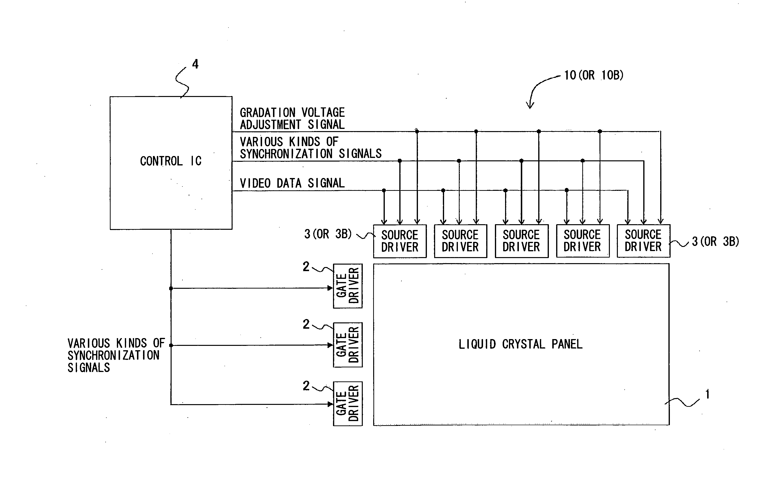
[0103]FIG. 1 is a block diagram illustrating an example of an arrangement of a liquid crystal display device according to Embodiment 1 of the present invention.

[0104] In FIG. 1, a liquid crystal display device 10 includes a liquid crystal panel 1, a plurality of gate drivers 2, a plurality of source drivers 3, and a control IC (control section) 4 for outputting a video data signal and control signals for controlling the gate drivers 2 and the source drivers 3.

[0105] The liquid crystal panel 1 is arranged so that: a plurality of scanning signal lines (gate signal lines) and a plurality of video signal lines (source signal lines) are provided so as to intersect with each other, and a plurality of display pixel sections are disposed in a matrix manner so that each of the display pixel sections is positioned in each of pixel areas (each of pixel sections) sectioned by both the signal lines and is connected to each gate signal line and each source signal line.

[0106] The gate drivers 2...

embodiment 2

[0153] The charge pull-in amount ΔV has a deviation in the panel face, so that there is a deviation (deviation in each gradation voltage) with respect to a value of a gradation voltage applied to a drain region of the TFT element. Generally, the deviation is referred to as “ω value”. As in Embodiment 1, all the gradation voltages VH0, VH63, VL0, and VL36 are increased / adjusted by the adjustment voltage Va having the same potential, thereby reducing the flicker. However, by making it possible also to correct the ω value with a gradation voltage adjustment function which allows the gradation voltage adjustment to be carried out more freely, it is possible to further greatly reduce the flicker.

[0154] Embodiment 2 will describe a liquid crystal display device 10B by which it is possible to correct the ω value which is a deviation in each gradation voltage.

[0155]FIG. 7 is a circuit diagram illustrating an example of an arrangement of a gradation voltage generation circuit 36B of a liqu...

embodiment 3

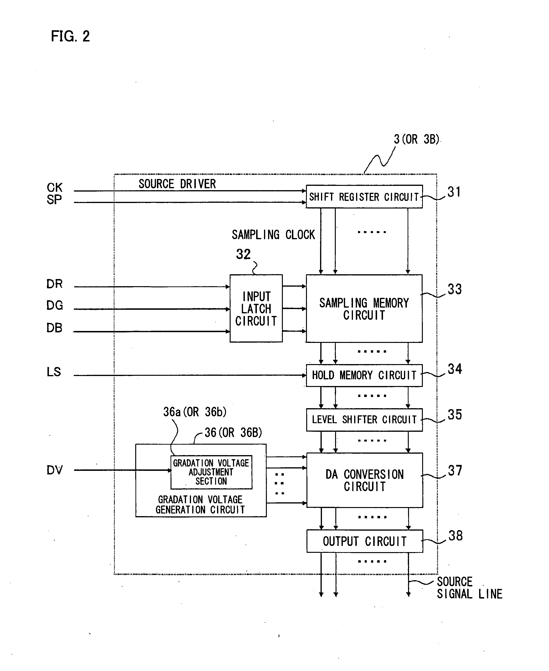
[0167] In the source driver 3 of FIG. 2, in order to add the gradation voltage adjustment function of the present invention, it is necessary to add at least one gradation voltage adjustment transmission line and at least one gradation voltage adjustment signal input terminal so as to transmit the gradation voltage adjustment signal DV. In case of supplying the gradation voltage adjustment signals DV from the control IC4 to the source drivers 3 respectively as in Embodiment 1 for example, it is necessary to add a transmission line and an input terminal. In case of supplying the gradation voltage adjustment signals DV0, DVX, and DV36 from the control IC4 as in Embodiment 2, it is necessary to add three transmission lines and three input terminals.

[0168] However, in view of a wiring condition of the driving circuit substrate, it is preferable not to increase the number of transmission lines and input terminals. Thus, Embodiment 3 describes a liquid crystal display device in which it i...


PUM


Abstract

A gradation voltage adjustment section for increasing a positive gradation voltage VHX of an X-th gradation and a negative gradation voltage of the X-th gradation so that the increment corresponds to a charge pull-in amount ΔV is provided in a gradation voltage generation circuit of each source driver. In at least one embodiment, a center value between the positive and negative gradation voltages is adjusted for each driver in accordance with a slant of the charge pull-in amount ΔV in a direction of a gate signal line, thereby suppressing a flicker without varying a gradation characteristic. Further, a center value between the positive and negative gradation voltages is adjusted for each horizontal line or for every plural lines in a single frame in accordance with a horizontal direction deviation and a vertical direction deviation of the charge pull-in amount ΔV in a transfer block, thereby suppressing a flicker without varying a gradation characteristic.

Description

TECHNICAL FIELD [0001] The present invention relates to (i) a liquid crystal display device such as an active matrix type liquid crystal display device used in a display screen such as a television device display, a personal computer monitor, and the like, and (ii) a liquid crystal display driving circuit used in the liquid crystal display device. BACKGROUND ART [0002] Conventionally, a liquid crystal display device includes a plurality of scanning signal lines (gate signal lines) and a plurality of video signal lines (source signal lines) which intersect with each other, and includes a liquid crystal panel having display pixel sections, disposed in a matrix manner, each of which is provided in each of areas sectioned by both the signal lines so as to be connected to each gate signal line and each source signal line. Each display pixel section includes: a liquid crystal capacitor Clc provided between a pixel electrode and a counter electrode; and a thin film transistor (TFT) whose g...

Claims


Application Information

Patent Timeline
Patent Type & Authority Applications(United States)
IPC IPC(8): G06F3/038
CPCG09G2310/027G09G3/3688
Inventor HIGASHINO, HIROYUKIUMEHARA, TETSUYAMORI, YASUKI
Owner SHARP KK
Why Eureka
Try Eureka