Display device and method of driving the same

a display device and matrix-type technology, applied in the direction of electric digital data processing, instruments, computing, etc., can solve the problems of flicker in display in liquid crystal panels, the transmittance of positive data voltage and negative data voltage is not perfectly symmetrical, and the accumulated charge cannot be held only by liquid crystal capacitance, so as to reduce the occurrence of flicker, suppress flicker, and reduce the cost

Active Publication Date: 2010-05-13
SHARP KK
View PDF10 Cites 23 Cited by
  • Summary
  • Abstract
  • Description
  • Claims
  • Application Information

AI Technical Summary

Benefits of technology

[0070]According to the first aspect of the present invention, the pixel formation portion pair of the first type and the pixel formation portion pair of the second type are repeated alternately in the extension direction of the video signal lines, and the pixel formation portion pair of the first type and the pixel formation portion pair of the second type are repeated in the extension direction of the scanning signal lines. Moreover, all of the polarities of video signals applied to each video signal line in each horizontal scanning period are set to be the same, and the polarity of a video signal applied to each video signal line is made vary between the case where a scanning signal line disposed on the upper side of any of the rows is selected and the case where a scanning signal line disposed on the lower side of any of the rows is selected. In such a manner, the polarities of the pixel voltages between the pixel formation portions neighboring in the horizontal direction and between the pixel formation portions neighboring in the vertical direction become opposite, thus the dot inversion driving is performed. Consequently, occurrence of flicker is suppressed. Moreover, while the pixel formation portion pair of the first type or the pixel formation portion pair of the second type is repeated in the extension direction of the scanning signal line, one video signal line is shared by the pixel formation portions disposed on both sides of the video signal line. Therefore, the number of video signal lines is smaller than that in the conventional configuration. Thus, occurrence of flicker is suppressed at low cost.
[0071]According to the second aspect of the present invention, in the display device in which the scan is performed sequentially, in a manner similar to the first aspect, occurrence of flicker can be suppressed while reducing the cost.
[0072]According to the third aspect of the present invention, in the display device in which the interlace driving is performed, in a manner similar to the first aspect, occurrence of flicker can be suppressed while reducing the cost.
[0073]According to the fourth aspect of the present invention, the common electrode driving method is the opposite AC driving. Consequently, the amplitude of a video signal to be applied to the video signal line can be made small. Therefore, the power consumption can be reduced. Moreover, since a video signal line drive circuit using a relatively low withstand voltage can be employed, the cost can be reduced.

Problems solved by technology

However, the accumulated charges cannot be held only by the liquid crystal capacitance, so that auxiliary capacitance is provided in parallel with the liquid crystal capacitance.
Generally, in an active matrix-type liquid crystal panel, since the characteristics of a switching element such as a TFT or the like provided for each pixel are insufficient, even when the positive and negative polarities of a drive video signal applied to a source bus line (application voltage using the potential of the common electrode as a reference) are symmetrical, the transmittance of the liquid crystal layer for positive data voltage and that for negative data voltage are not perfectly symmetrical.
Consequently, in the driving method (frame inversion driving method) for inverting the positive / negative polarity of a voltage applied to the liquid crystal frame by frame, flicker occurs in display in a liquid crystal panel.
However, according to the line inversion driving method, suppression of flicker is insufficient.
Consequently, in the case of employing the opposite DC driving, a source driver having a large withstand voltage is required and power consumption becomes large.

Method used


Image

  • Display device and method of driving the same
  • Display device and method of driving the same
  • Display device and method of driving the same

Examples


first embodiment

1. First Embodiment

1.1 General Configuration and Operation

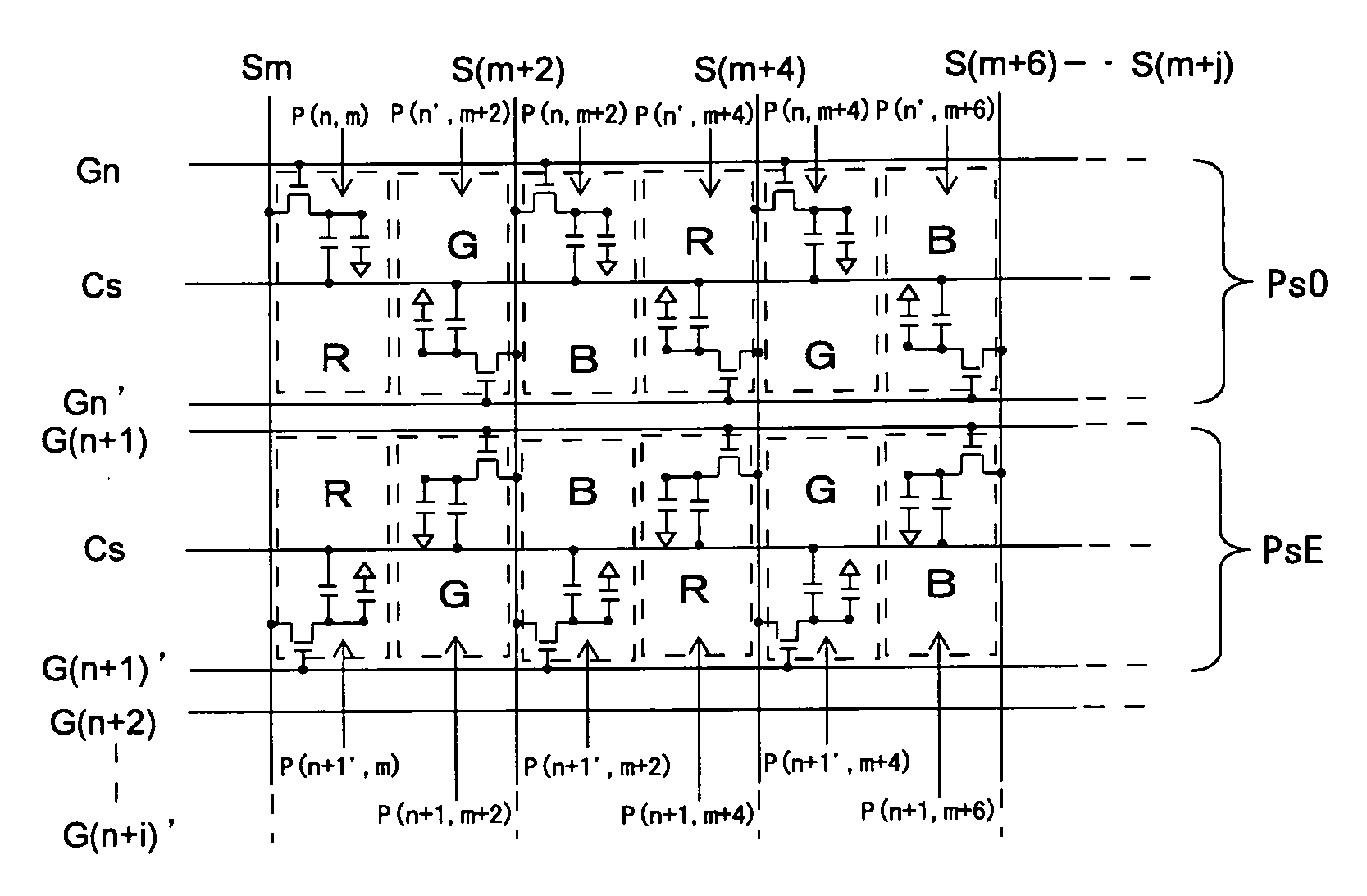
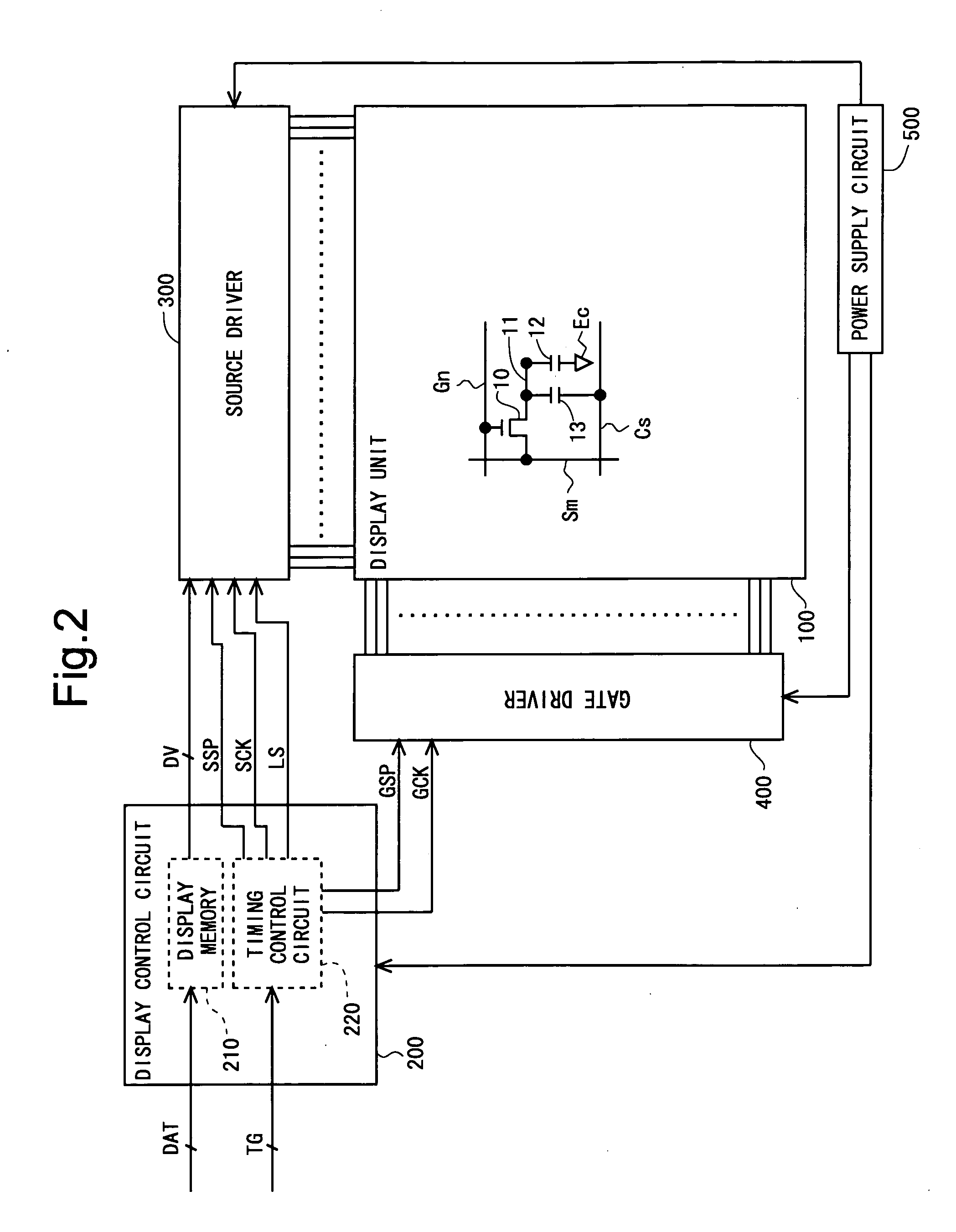
[0141]FIG. 2 is a block diagram showing a general configuration of a liquid crystal display device according to a first embodiment of the present invention. The liquid crystal display device has a display unit 100, a display control circuit 200, a source driver (video signal line drive circuit) 300, a gate driver (scanning signal line drive circuit) 400, and a power supply circuit 500. The display control circuit 200 includes a display memory 210 and a timing control circuit 220. Note that, the liquid crystal display device will be described on assumption that it is of the QVGA type.

[0142]The display unit 100 includes a plurality of source bus lines (video signal lines), a plurality of gate bus lines (scanning signal lines), and a plurality of pixel formation portions. The plurality of pixel formation portions are classified into an R pixel formation portion for forming a pixel (sub-pixel) of red, a G pixel formation portion ...

second embodiment

2. Second Embodiment

2.1 About an Array of Pixels

[0173]The general configuration of a liquid crystal display device according to a second embodiment of the present invention is similar to that of the first embodiment, so that it will not be described. FIG. 17 is an equivalent circuit diagram showing the configuration of a part of the display unit 100 in the embodiment. In the embodiment, the array of pixels is different from that of the first embodiment (see FIG. 1). The n-th row and the (n+1)th row have similar configurations, and the (n+2)th row and the (n+3)th row have similar configurations.

[0174]In the n-th row and the (n+1)th row, with respect to the sub-pixel disposed on the left side out of the two sub-pixels disposed between neighboring two source bus lines, the gate terminal of the TFT 10 is connected to the gate bus line disposed on the upper side of the sub-pixel, and with respect to the sub-pixel disposed on the right side, the gate terminal of the TFT 10 is connected to...

third embodiment

3. Third Embodiment

3.1 About an Array of Pixels

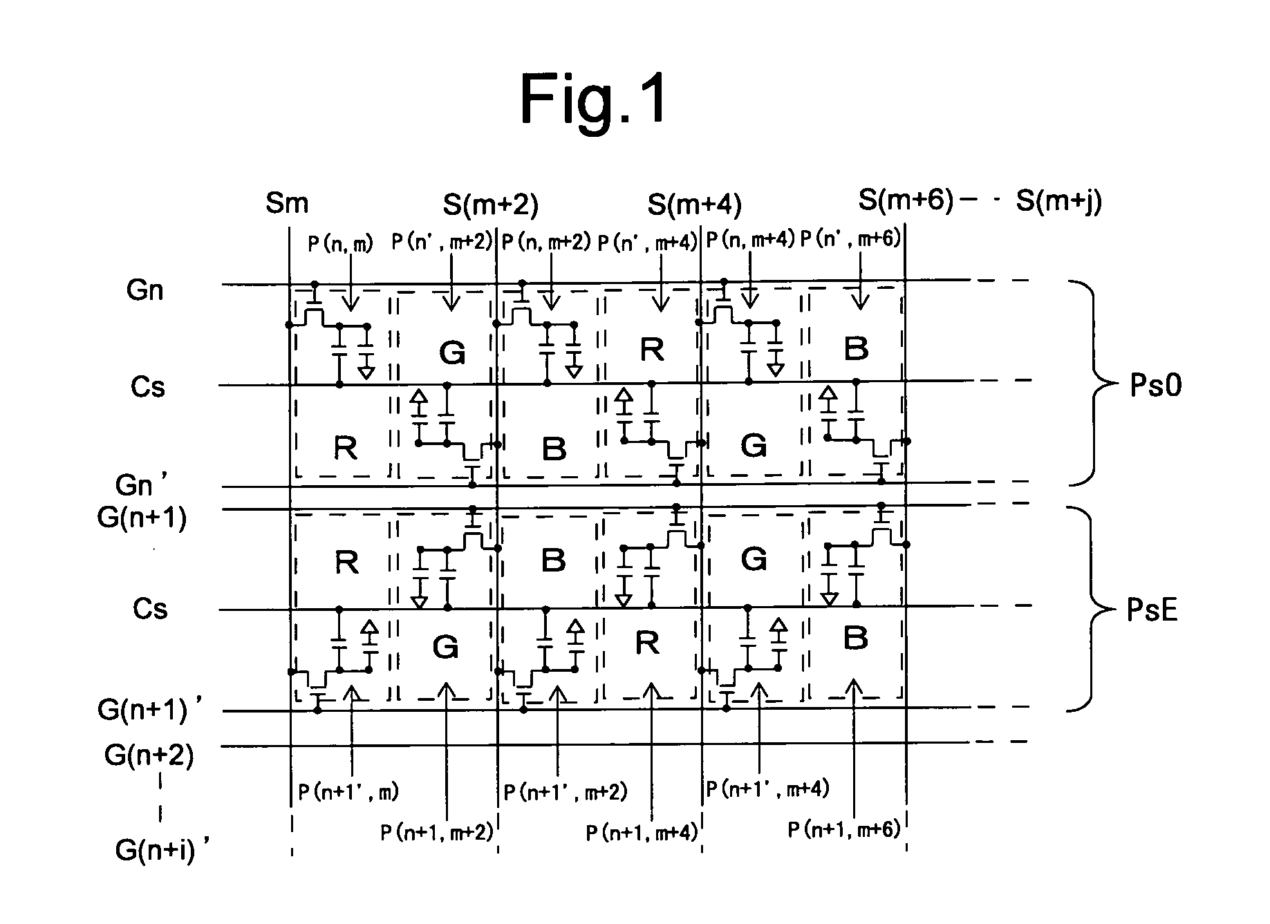
[0193]The general configuration of a liquid crystal display device according to a third embodiment of the present invention is similar to that of the first embodiment, so that it will not be described. FIG. 27 is an equivalent circuit diagram showing the configuration of a part of the display unit 100 in the embodiment. In the embodiment, the array of pixels in the odd-numbered rows PsO is similar to that of the first embodiment shown in FIG. 1. On the other hand, the array of pixels in the even-numbered rows PsE is different from that of the first embodiment. In the embodiment, the array of pixels in the odd-numbered rows PsO and the array of pixels in the even-numbered rows PsE are similar to each other.

3.2 Driving Method

[0194]FIG. 28 is a signal waveform chart for explaining a driving method in the embodiment. To gate bus lines, an active scanning signal is sequentially applied one-horizontal-scanning-period by one-horizontal-scannin...


PUM


Abstract

In one embodiment of the present invention, an active-matrix type display unit, and a drive method thereof are disclosed. Gate-bus lines are provided at both top and bottom sides of each row. Two sub-pixels are formed at a region surrounded by two adjacent source-bus lines and two adjacent gate-bus lines. At the odd-numbered rows, for the left-side sub-pixel of those two sub-pixels, a scanning signal is supplied from the top-side gate-bus line, while a video signal is supplied from the left-side source-bus line. For the right-side sub-pixel, on the contrary, a scanning signal is supplied from the bottom-side gate-bus line, while a video signal is supplied from the right-side source-bus line. At the even-numbered rows, the gate-bus line from which a scanning signal is supplied is reversed to the case of the odd-numbered rows. The gate-bus lines are sequentially selected one by one, and all the video signal polarities are made the same during each horizontal scanning period.

Description

TECHNICAL FIELD[0001]The present invention relates to an active matrix-type display device and a method of driving the same.BACKGROUND ART[0002]Conventionally, an active matrix-type liquid crystal display device having a TFT (Thin Film Transistor) as a switching element is known. The liquid crystal display device includes a liquid crystal panel constructed by two insulating substrates which face each other. On one of the substrates of the liquid crystal panel, gate bus lines (scanning signal lines) and source bus lines (video signal lines) are provided in a lattice shape, and TFTs are provided near the crossing points of the gate bus lines and the source bus lines. The TFT is configured by a gate electrode, a source electrode, and a drain electrode. The gate electrode is connected to the gate bus line, the source electrode is connected to the source bus line, and the drain electrode is connected to any of pixel electrodes disposed in a matrix on the substrate for forming an image. O...

Claims


Application Information

Patent Timeline
Patent Type & Authority Applications(United States)
IPC IPC(8): G09G5/10G09G3/36
CPCG09G3/3607G09G2300/0426G09G3/3648G09G3/3614
Inventor MURAI, ATSUHITOTAKAHASHI, KOZO
Owner SHARP KK
Why Eureka
Try Eureka