Check patentability & draft patents in minutes with Patsnap Eureka AI!

Electronic device shell and manufacture method thereof

A technology for electronic devices and manufacturing methods, applied in the fields of electrical equipment shells/cabinets/drawers, decorative art, telephone communications, etc., can solve the problems that the shell is not suitable for in-mold decoration molding, etc., and achieve simple manufacturing methods, beautiful shells, Applicable to a wide range of effects

Inactive Publication Date: 2010-11-10
SHENZHEN FUTAIHONG PRECISION IND CO LTD
View PDF0 Cites 4 Cited by
  • Summary
  • Abstract
  • Description
  • Claims
  • Application Information

AI Technical Summary

Problems solved by technology

Therefore, the shell of this kind of electronic device is not suitable to adopt the method of in-mold decoration molding.

Method used


Image

  • Electronic device shell and manufacture method thereof
  • Electronic device shell and manufacture method thereof
  • Electronic device shell and manufacture method thereof

Examples


Embodiment Construction

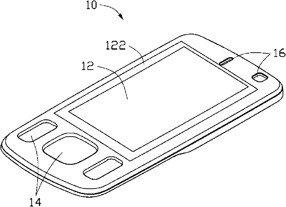
[0017] see figure 1 , a preferred embodiment of the present invention an electronic device casing 10 is formed with a window 12 , a plurality of button holes 14 and a plurality of function holes 16 . The window 12 is in the shape of a rectangular frame. A window ink printing area 122 is formed around the window 12 . The window ink printing area 122 is used to print the window ink layer to form the window 12 . The button hole 14 is formed at one end of the window 12 for assembling a button of an electronic device. The function hole 16 is formed at the other end opposite to the button hole 14, and is used to communicate with the outside world from the functional elements assembled inside the electronic device, such as matching with a camera or a receiver device.

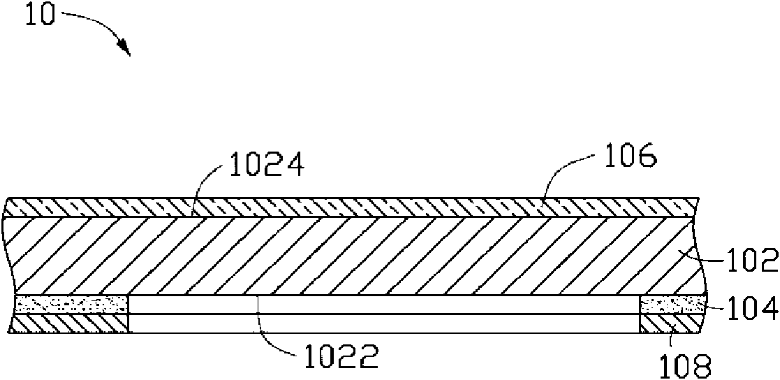
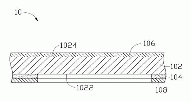
[0018] see figure 2 , the electronic device casing 10 includes a transparent base casing 102 , a window ink layer 104 , a transparent ink layer 106 and a primer layer 108 . The transparent base case 102 is formed i...


PUM


Abstract

The invention relates to an electronic device shell which comprises a transparent base shell and a window ink layer, wherein the transparent base shell is formed by injection, and the window ink layer is coated on the inner surface of the transparent base shell to form a window on the transparent base shell. The invention also discloses a manufacture method of the electronic device, which comprises the steps of: firstly, forming the base shell of the electronic shell by injection; and secondly, forming the window on the window ink layer printed on the inner surface layer of the base shell. The manufacture method of the electronic shell has simple operation and can effectively protect the ink layer of the shell window.

Description

technical field [0001] The present invention relates to an electronic device housing and its manufacturing method, in particular to an electronic device housing with a window and its manufacturing method. Background technique [0002] With the use and popularization of electronic devices, consumers have higher and higher requirements on the appearance of electronic devices. Existing electronic device casings with windows generally adopt the method of making each component separately and then assembling them. The manufacturing process is to first make a base shell and a window frame, and then assemble the window frame and the base shell by hot-melting or pasting. As a whole, there is a gap between the window frame and the base shell of the electronic device housing prepared by this method, and the window frame and the base shell may be separated after a long time of use, which is not durable, the overall aesthetics of the electronic device is poor, and the manufacturing proce...

Claims


Application Information

Patent Timeline
Patent Type & Authority Applications(China)
IPC IPC(8): H05K5/00H04M1/02B44C1/00
CPCH04M1/0283H05K5/0243Y10T428/13
Inventor 祝金强张小兵赫英雷申玉奇
Owner SHENZHEN FUTAIHONG PRECISION IND CO LTD
Features
  • R&D
  • Intellectual Property
  • Life Sciences
  • Materials
  • Tech Scout
  • Unparalleled Data Quality
  • Higher Quality Content
  • 60% Fewer Hallucinations
Learn More