Support for testing BGA packaged chips

A technology for installing chips and chips, which is applied in the field of BGA packaging chip test support, can solve the problems of inability to locate the chip soldering, whether the test chip is qualified, etc.

Inactive Publication Date: 2010-12-01
CHONGQING UNIV OF POSTS & TELECOMM
View PDF7 Cites 13 Cited by
  • Summary
  • Abstract
  • Description
  • Claims
  • Application Information

AI Technical Summary

Problems solved by technology

However, the number of pins of BGA packaged chips on the market, the distance between pins, and the package shape are different, so that users (especially those engaged in research or small-scale production users) when purchasing corresponding BGA packaged chips And before welding, it is impossible to test whether the chip is qualified by non-welding method. When there is a problem in the circuit board welding manufacturing process, it is impossible to locate whether it is a problem with the chip itself or a welding problem (because it is difficult to test whether the BGA package is welded or not with ordinary equipment and methods); There is no test device related to BGA packaged chips on the market, and there is no record of a BGA packaged chip test device that can be applicable to various pin numbers, distances between pins and package shapes in the prior art

Method used


Image

  • Support for testing BGA packaged chips
  • Support for testing BGA packaged chips
  • Support for testing BGA packaged chips

Examples


Embodiment Construction

[0026] In order to make the purpose, technical solution and advantages of the present invention clearer, the BGA packaged chip test support of the present invention will be further described in detail below in conjunction with the accompanying drawings and embodiments.

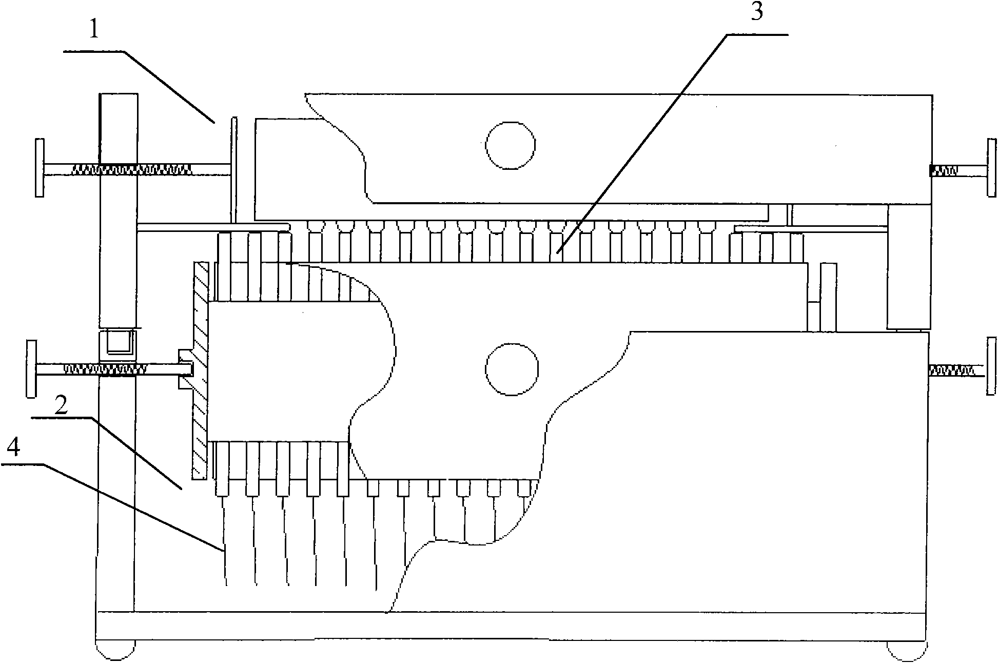
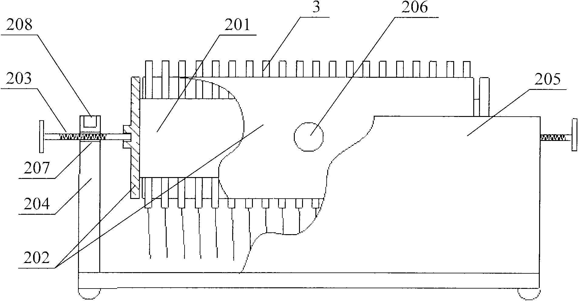
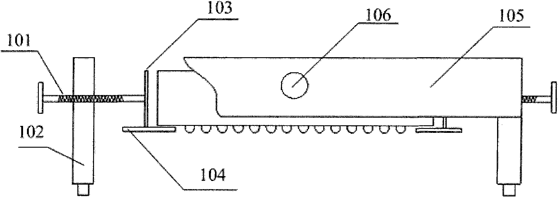
[0027] Such as figure 1 , figure 2 and image 3 Shown, as a kind of preferred embodiment, BGA package chip test support of the present invention mainly comprises:

[0028] Chip holder 1, probe holder 2 and test probe 3, chip holder 1 and probe holder 2 are clamped, that is, chip holder 1 and probe holder 2 are two separate parts, through the fixing pillar Snap together; the test probe 3 passes through the probe holder 2, one end is connected to the metal lead 4, and the other end is used to contact the solder joint of the chip. When the chip holder 1 and the probe holder 2 are snapped together , the other end of the test probe 3 will be in contact with the solder joint of the chip, and the test signal will...


PUM


Abstract

The invention provides a support for testing BGA packaged chips, belonging to the field of packaged chip testing. The support comprises a chip fixing frame, a probe fixing frame and test probes, wherein the chip fixing frame and the probe fixing frame are clamped; the test probes run through the probe fixing frame; one end of the test probes is connected with metal leads and the other end thereof is used for contacting welding spots of the chips; the chip fixing frame can not only fix the chips to be tested but also adjust the chip positions in the horizontal or upper and lower directions; and the probe fixing frame can adjust the area of a probe fixing block by adjusting push plates and further adjust the distance between the probes. Thus the support can not only conveniently realize testing the BGA packaged chips on a large scale but also carry out flexible adjustment and accurate matching and fixing according to the pin quantity and sizes of the chips to be tested and is suitable for the BGA packaged chips with various pin quantities and sizes.

Description

technical field [0001] The invention relates to the field of packaging chip testing, in particular to a BGA (Ball Grid Array, ball grid array) packaging chip testing support. Background technique [0002] BGA was developed in the 1990s with the advancement of integration technology, the improvement of equipment, and the use of deep submicron technology. A new packaging technology has emerged. Chips packaged with BGA technology can make the chip have smaller volume, better electrical performance, faster speed and better heat dissipation performance without changing the function. Now more and more chips are packaged in BGA . BGA packaged chips have a wide range of application requirements in embedded devices, portable devices and handheld computers. However, the number of pins of BGA packaged chips on the market, the distance between pins, and the package shape are different, so that users (especially those engaged in research or small-scale production users) when purchasin...

Claims


Application Information

Patent Timeline
Patent Type & Authority Applications(China)
IPC IPC(8): G01R1/04
Inventor 曾垂省向浏欣梁亦龙舒坤贤梁晓艳
Owner CHONGQING UNIV OF POSTS & TELECOMM
Why Eureka
Try Eureka