Semiconductor device having grooved leads to confine solder wicking
A semiconductor and lead technology, applied in the direction of semiconductor devices, semiconductor/solid-state device manufacturing, semiconductor/solid-state device components, etc., can solve problems such as difficulty in containing solder wicking
- Summary
- Abstract
- Description
- Claims
- Application Information
AI Technical Summary
Problems solved by technology
Method used
Image

Examples
Embodiment Construction
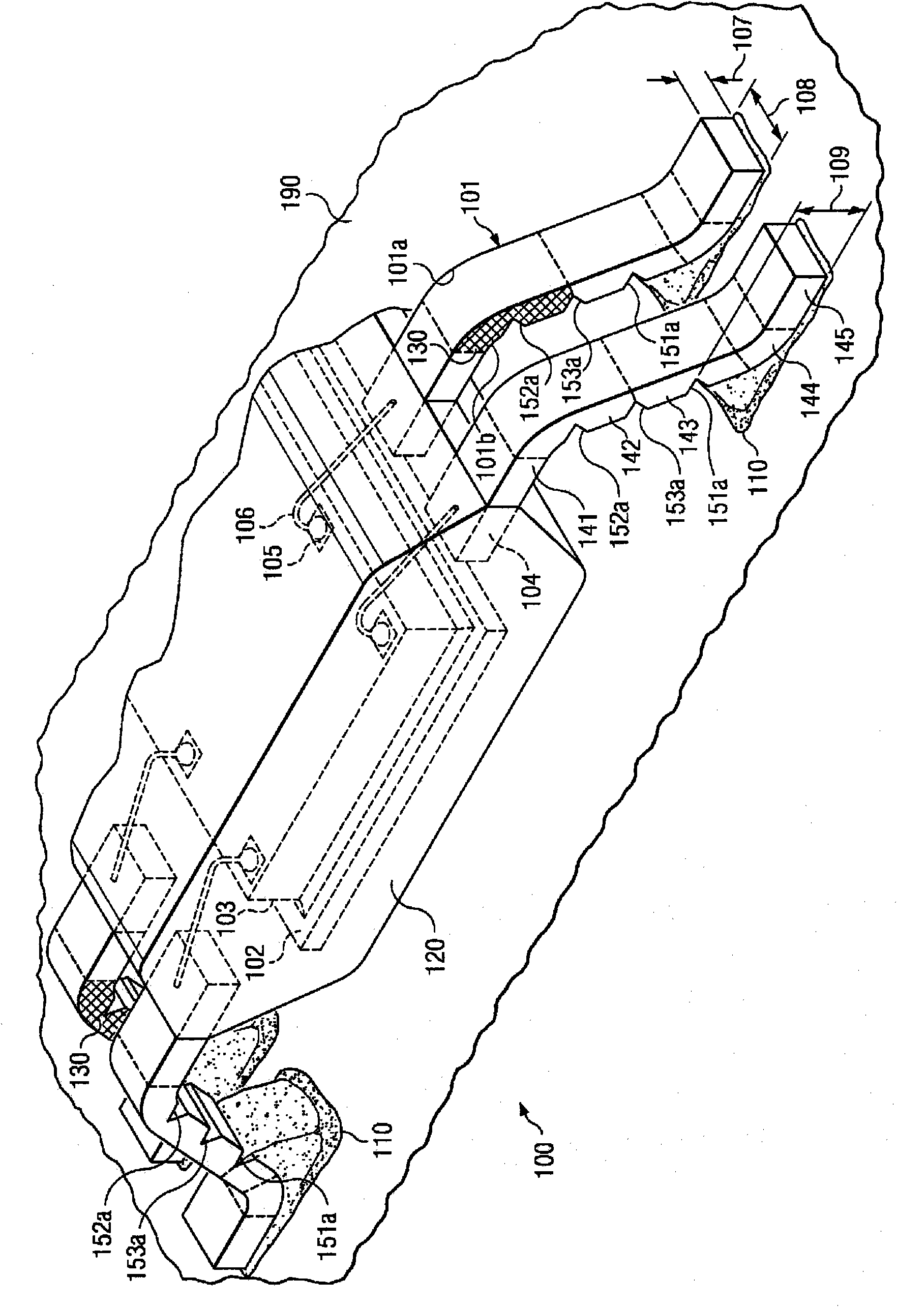
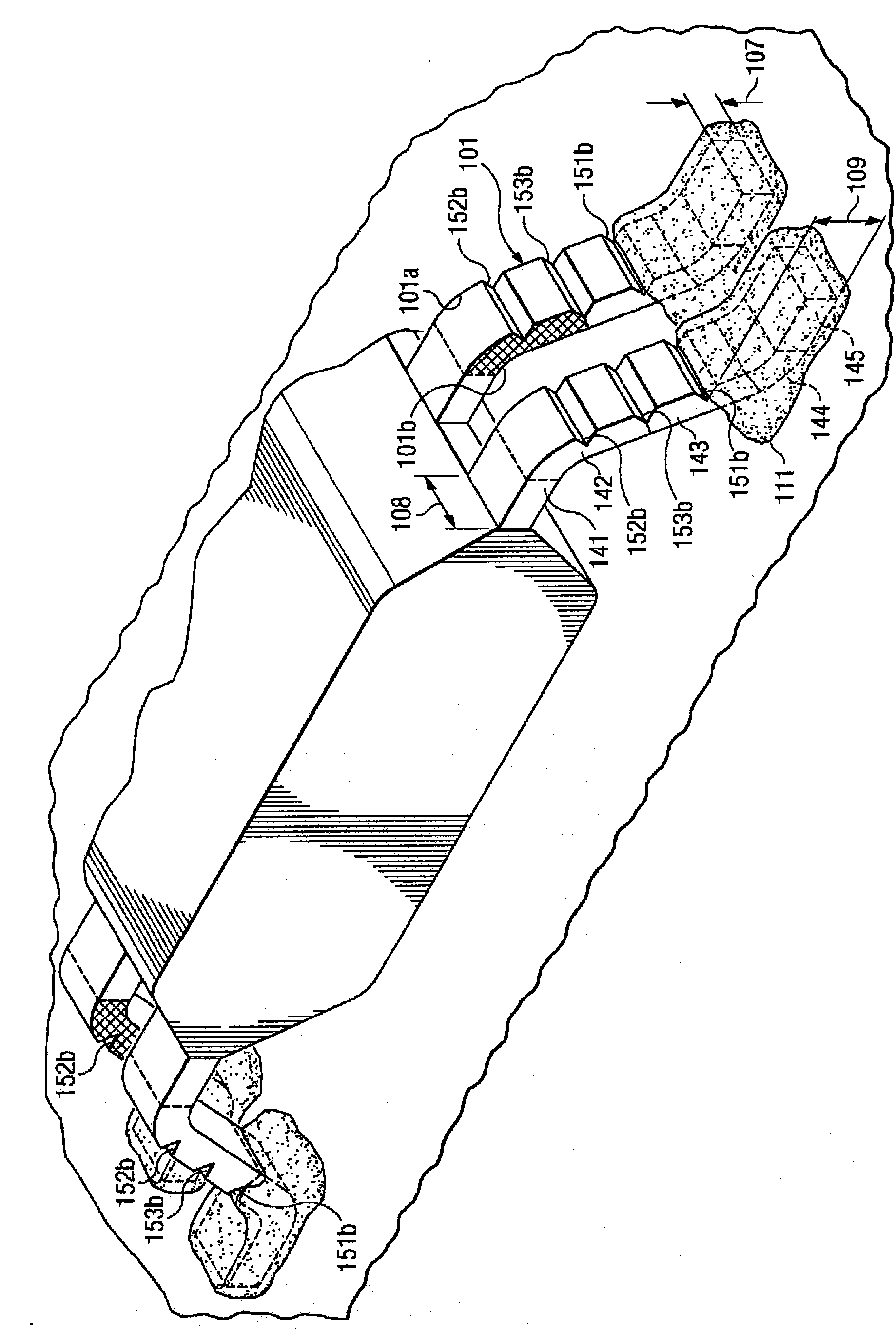
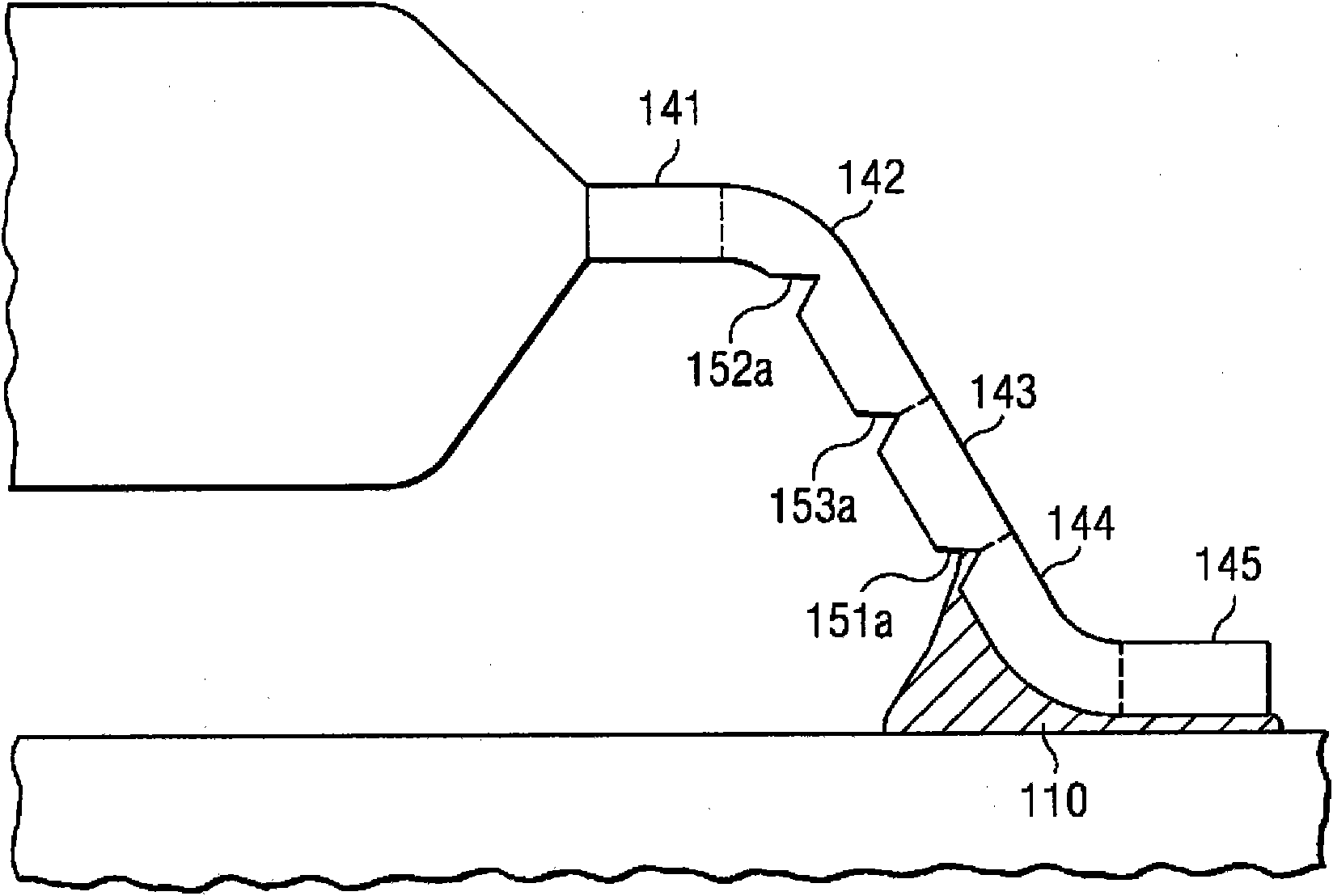
[0022] figure 1 An exemplary embodiment of the invention is illustrated. figure 1 Depicts a portion of a semiconductor device (generally designated 100 ) belonging to the surface mount product family. These devices have an insulating package 120 with a protruding metal segment 101 outside the package 120 and thus called the outer segment 101 . The outer segment is shaped and formed to attach to the surface of a substrate or board 190 using solder 110; figure 1 The shape illustrated in is often referred to as the "gull wing" shape. After surface mount device solder attachment to the substrate, it is easy to visually inspect all solder reflow sites to confirm defect-free attachment and contact - a major reason why surface mount devices are so popular in the semiconductor industry.
[0023] The metal portion of device 100 includes: pad 102 for firmly positioning semiconductor chip 103 ; metal outer segment 101 ; and metal segment 104 located inside package 120 ("inner" segment...
PUM
 Abstract
Description
Claims
Application Information
 - R&D Engineer
- R&D Manager
- IP Professional
- Industry Leading Data Capabilities
- Powerful AI technology
- Patent DNA Extraction
Browse by: Latest US Patents, China's latest patents, Technical Efficacy Thesaurus, Application Domain, Technology Topic.
© 2024 PatSnap. All rights reserved.Legal|Privacy policy|Modern Slavery Act Transparency Statement|Sitemap