

Circuit substrate, an electronic device arrangement and a manufacturing process for the circuit substrate
a technology of electronic devices and circuit substrates, which is applied in the manufacture of printed circuits, printed circuit aspects, basic electric elements, etc., can solve the problems of density growth of wiring density, and achieve excellent workability and reliability, and high speed transmission characteristics
- Summary
- Abstract
- Description
- Claims
- Application Information
AI Technical Summary
Benefits of technology
Problems solved by technology
Method used
Image

Examples
first embodiment
First, the present invention will be explained.
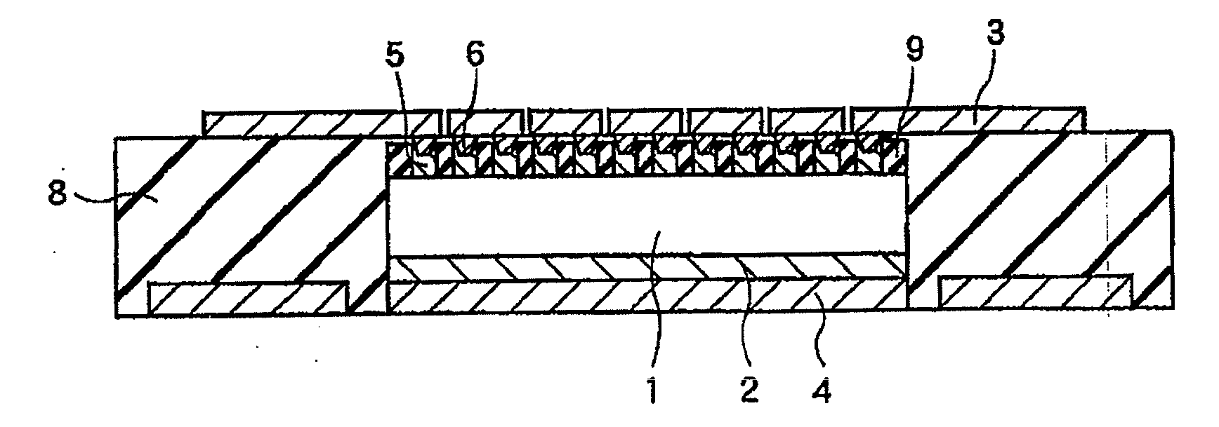
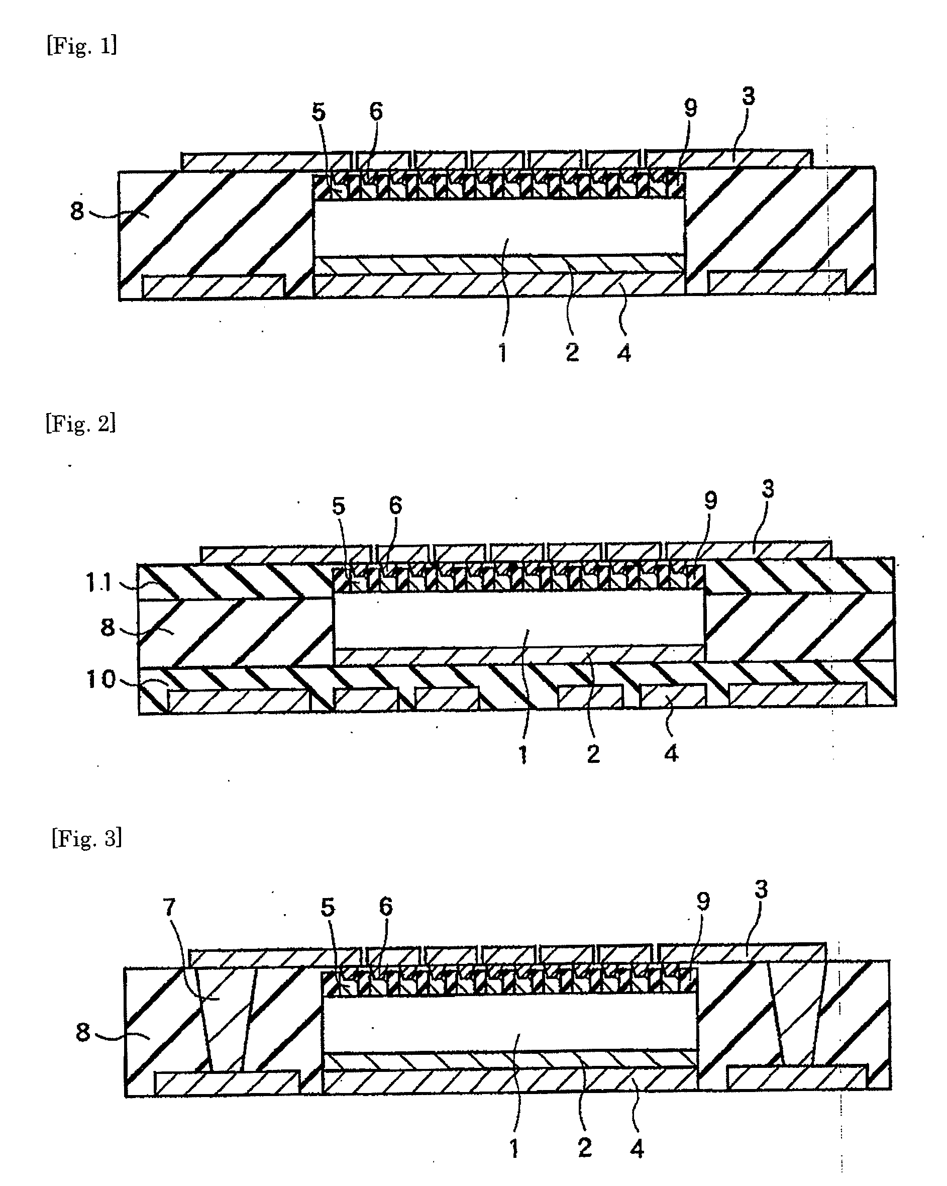
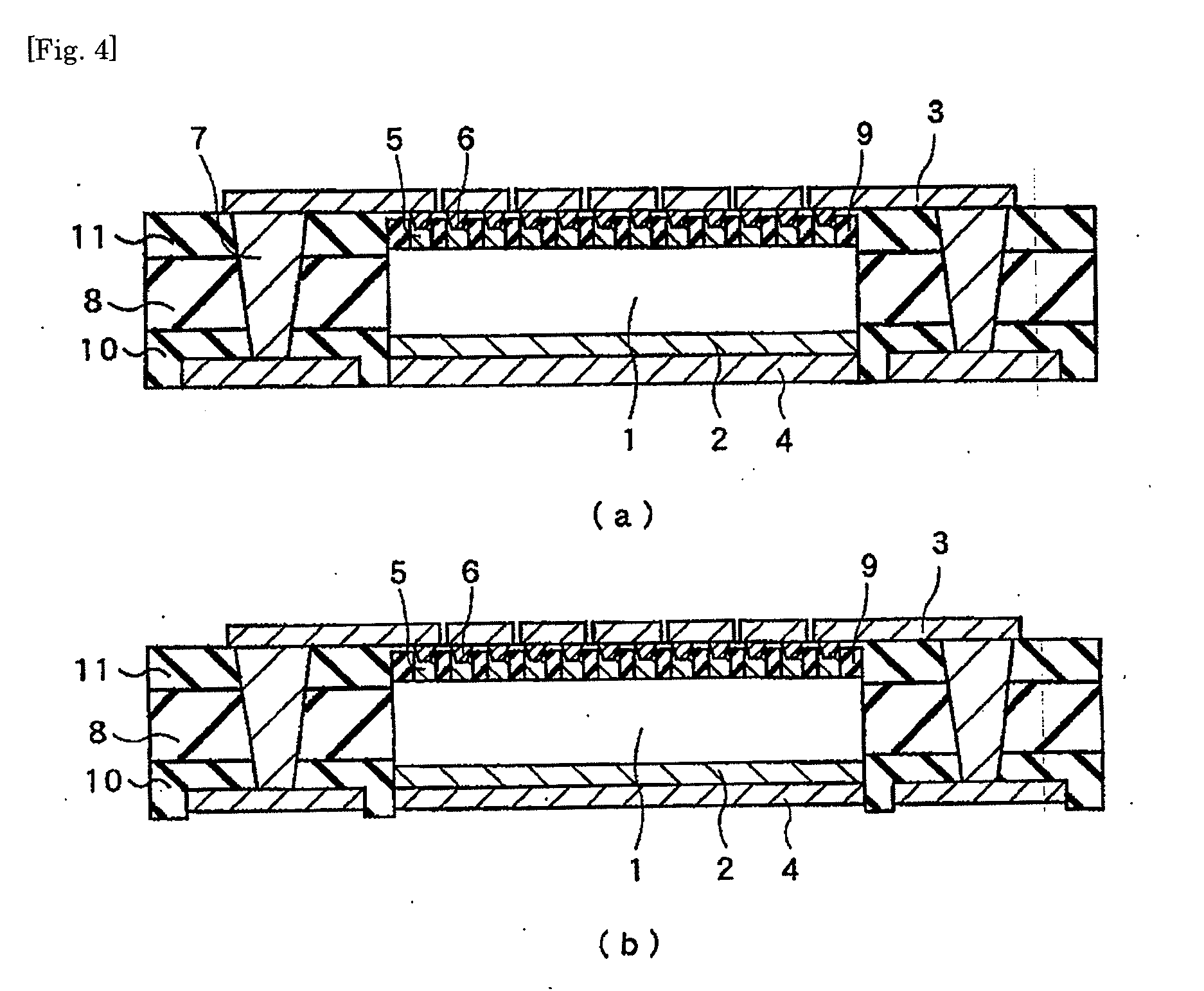
FIG. 1 is a schematic sectional view illustrating a circuit substrate according to the first embodiment of the present invention. In the circuit substrate according to the first embodiment, a function element 1 having an electrode terminal 5 and an insulating resin layer 9 on its surface is sealed in an insulating resin layer 8 as a base member of the circuit substrate. A conductive wiring 3 formed on the surface of the insulating resin layer 8, and the electrode terminal 5 of the function element 1 is connected through a conductive via 6. Further, the rear face of the function element 1 and a conductive wiring 4 formed on the rear face of the insulating resin layer 8 with exposed are bonded inside the insulating resin layer 8 by an adhesion layer 2.
In FIG. 1, the surface exposing outside the conductive wiring 4 is disposed in the same plane with the rear face of the insulating resin layer 8. However, in the present embodiment, the surf...
PUM
 Abstract
Description
Claims
Application Information