Miniaturized microwave antenna

a microwave antenna and miniaturized technology, applied in the direction of resonant antennas, substantially flat resonant elements, elongated active element feed, etc., can solve the problems of expensive contacts, inability to directly solder .lambda./4 monopoles to printed circuit boards, and considerable disadvantages

Inactive Publication Date: 2004-01-20
KONINKLIJKE PHILIPS ELECTRONICS NV
View PDF4 Cites 126 Cited by
  • Summary
  • Abstract
  • Description
  • Claims
  • Application Information

AI Technical Summary

Problems solved by technology

Particular problems then arise especially with the use of electronic components in the high-frequency and microwave technology fields, because many properties of the components are dependent on their physical dimensions.
Since these dipole antennas are too large for many applications, however, in particular for mobile telecommunication (the wavelength for the GSM900 range is, for example, approximately 32 cm), alternative antenna structures are utilized.
Although antennas of this type are widely used, they do have considerable disadvantages.
Furthermore, the .lambda. / 4 monopoles cannot be directly soldered onto the printed circuit board because the wire antennas are mostly used as pull-out members, for example in mobile telephones.
This means that expensive contacts are necessary for the information exchanged between the printed circuit board and the antenna.
A further disadvantage of antennas of this type is the mechanical instability of the antenna itself as well as the adaptation of the housing to the antenna made necessary by this instability.
If a mobile telephone, for example, is dropped, the antenna will usually break off, or the housing is damaged in that location where the antenna can be pulled out.
These antennas, however, have the disadvantage that at least portions of the conductor tracks extend inside the substrate, and that accordingly the substrate is to be manufactured in several layers and with a certain minimum size, which may be comparatively expensive.
In addition, it is not possible with this arrangement of the conductor tracks to carry out an electrical adaptation of the conductor tracks to a concrete constructional situation in the finished state, because the conductor track is no longer accessible, or only partly accessible.
It was also found that passive circuits for impedance adaptation are unnecessary, because such an adaptation can be achieved through a change in the fully accessible metallization (for example achieved by laser trimming) with the antenna in the incorporated state.

Method used


Image

  • Miniaturized microwave antenna
  • Miniaturized microwave antenna
  • Miniaturized microwave antenna

Examples


first embodiment

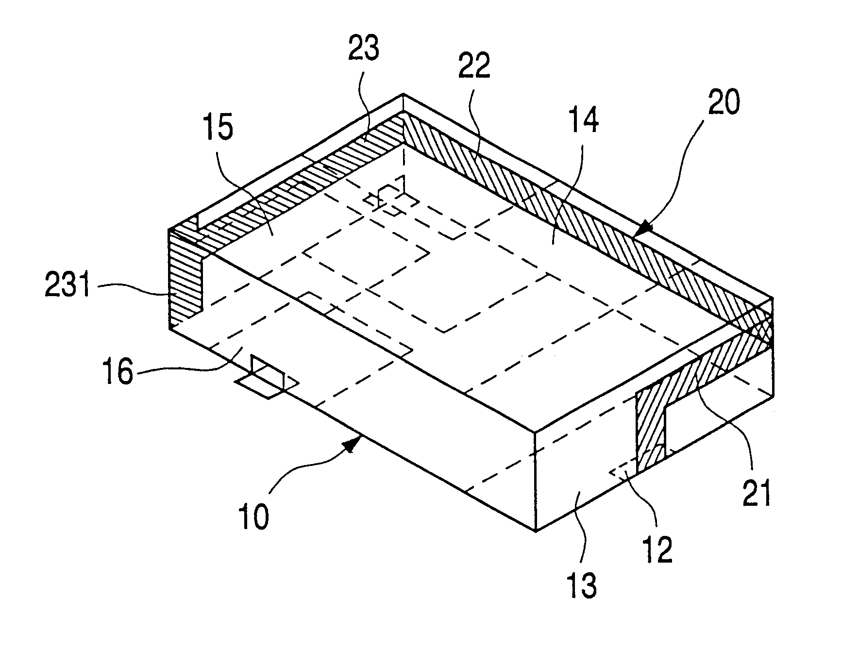
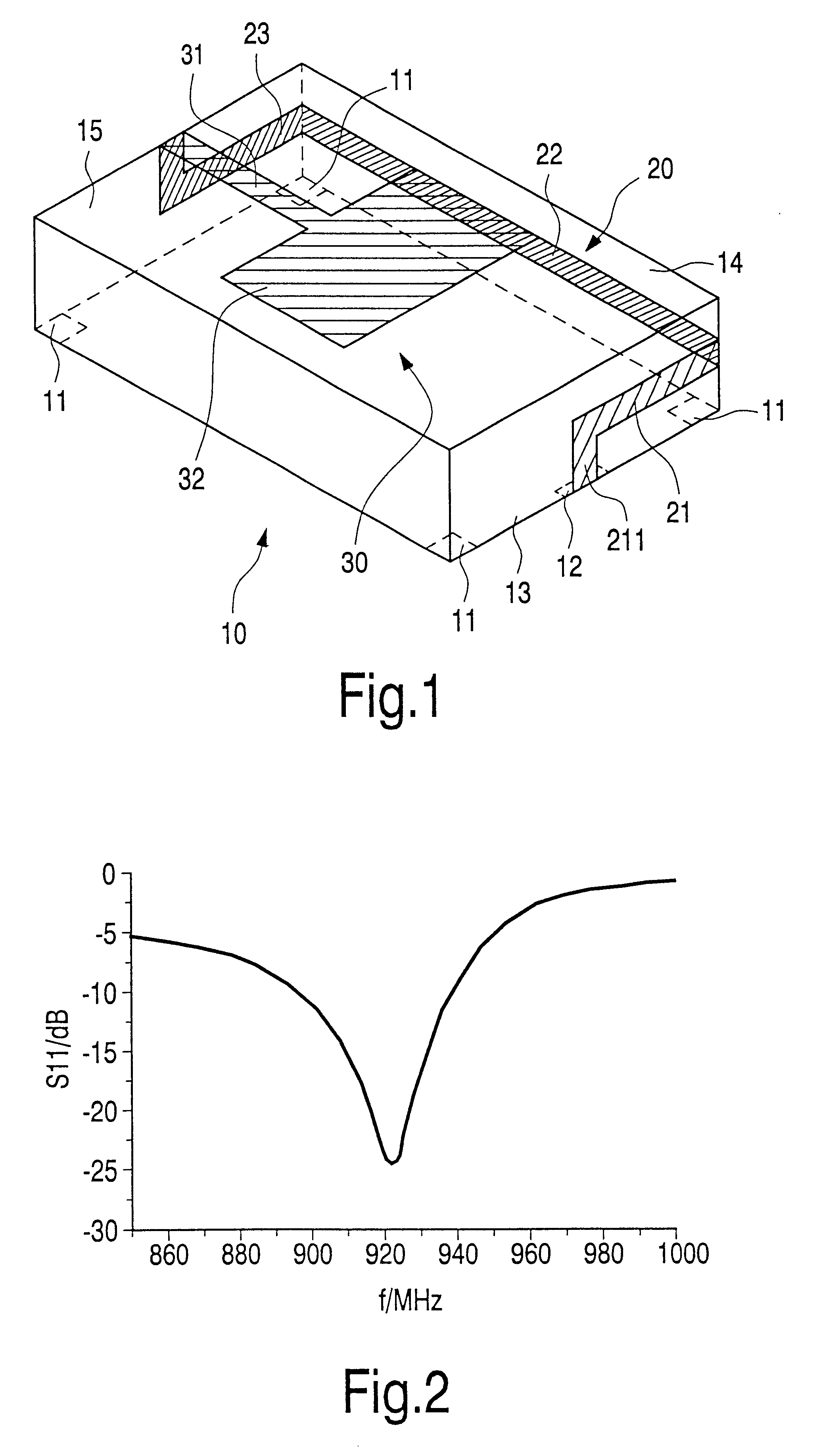
More in detail, a first embodiment shown in FIG. 1 shows a rectangular block-shaped substrate 10 with a resonant conductor track structure 20, 30. The substrate 10 is provided with several soldering points 11, by which it can be soldered on a printed circuit board by surface mounting (SMD technology), at the corners of its lower surface. Furthermore, a feed terminal 12 is present at the lower side in the central region of a first side face 13 in the form of a metallization pad which is soldered to a corresponding conductor region on a printed circuit board during mounting and through which the antenna is supplied with electromagnetic energy to be radiated. Starting from the feed terminal 12, a first portion 21 of a conductor track 20 extends vertically to approximately halfway the height of the first side face 13 and then continues in horizontal direction along the first side face 13 to a second side face 14. The conductor track then continues in horizontal direction along the secon...

second embodiment

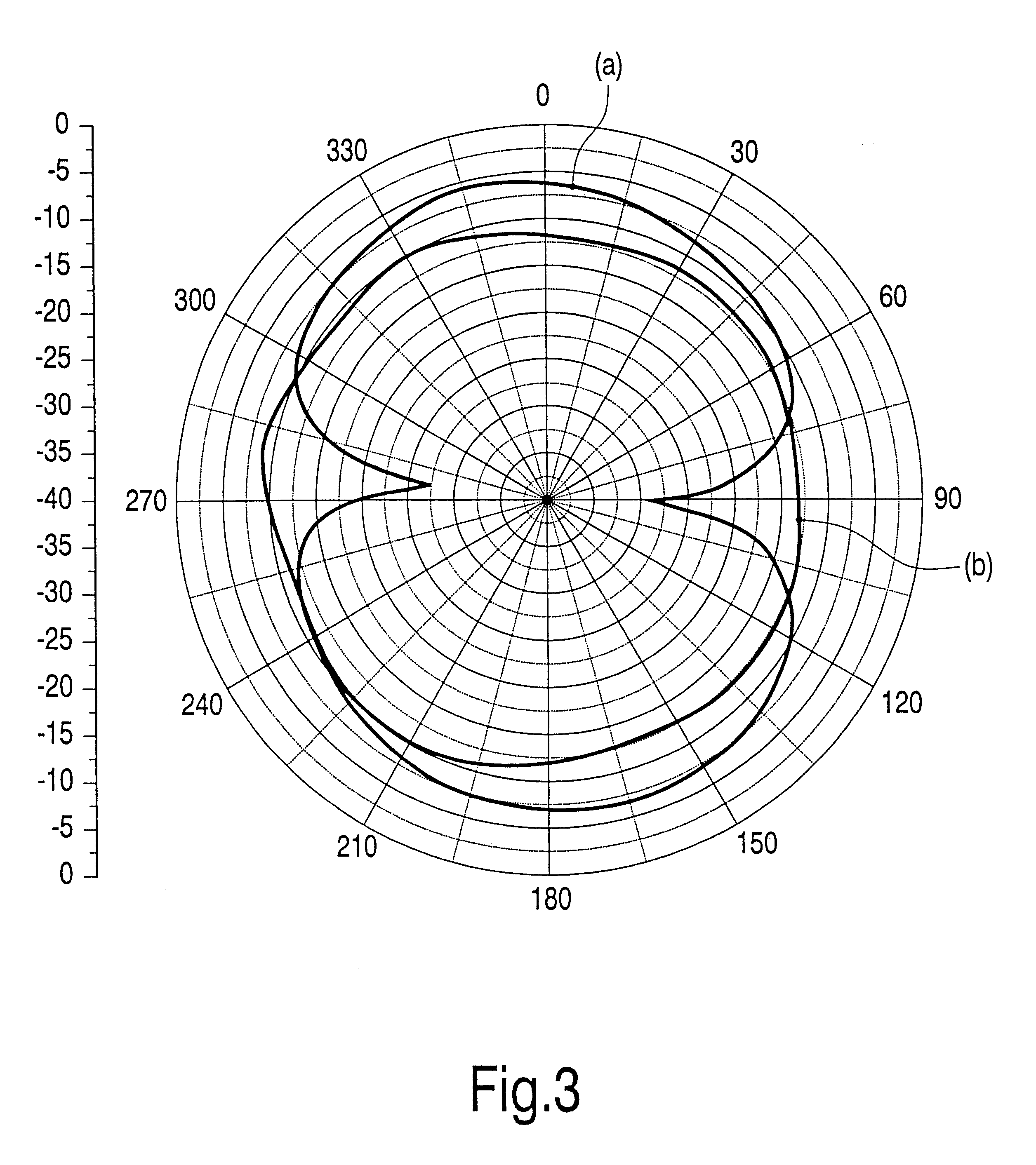
This second embodiment of the antenna can also be mounted on a printed circuit board by surface mounting (SMD technology). Furthermore, a very homogeneous, quasi-omnidirectional space pattern both in horizontal direction and in the direction perpendicular thereto can be achieved again.

It was also found that two resonance frequencies are excited if the two metallization structures 30, 40 are slightly different, i.e. have different lengths or widths, with different couplings (for example by a gap 211 of variable width and / or length) to the joint conductor track 20, or with different dimensions of the first and second metallization pads 33, 43, which frequencies are mutually shifted in accordance with these differences. In that case, for example, the first metallization structure 30 will have a somewhat lower resonance frequency than the second metallization structure 40.

The number of these resonances can be increased in that, for example, one or several further substrates with identic...


PUM


Abstract

A miniaturized antenna is described with at least a ceramic substrate (10) and a metallization, particularly designed for use in the high-frequency and microwave ranges. The antenna is characterized in that the metallization is a surface metallization which is formed by a feed terminal (12) for electromagnetic energy to be radiated, by at least a first metallization structure (30), and by a conductor track (20) extending along at least part of the circumference of the substrate (10), which track connects the feed terminal to the at least one first metallization structure (30), which first metallization structure (30) comprises a first conductor track portion (31) extending from a side of the substrate lying opposite the feed terminal (12) towards the feed terminal and a first metallization pad (32). The antenna can be provided on a printed circuit board by surface mounting and has a great impedance and radiation bandwidth, so that it is particularly suitable for use in mobile telephones operating in the GSM and UMTS bands.

Description

1. Field of the InventionThe invention relates to a miniaturized antenna with at least a ceramic substrate and a metallization, in particular for use in the high-frequency and microwave range. The invention further relates to a printed circuit board and a mobile telecommunication device with such an antenna.2. Description of the Related ArtFollowing the trend towards ever smaller electronic components, in particular in the field of telecommunication technology, all manufacturers of passive and / or active electronic components are intensifying their activities in this field. Particular problems then arise especially with the use of electronic components in the high-frequency and microwave technology fields, because many properties of the components are dependent on their physical dimensions. This is based on the generally known fact that the wavelength of the signal becomes smaller with increasing frequency, which again has the result that the supplying signal source is influenced in ...

Claims


Application Information

Patent Timeline
Patent Type & Authority Patents(United States)
IPC IPC(8): H01Q1/38H01Q1/24H01Q9/04H01Q5/00H05B6/72H01Q1/36H01Q5/357H01Q5/40H01Q9/30H01Q9/40H01Q13/08
CPCH01Q1/243H01Q1/38H01Q5/40H01Q21/30H01Q5/357H01Q9/045H01Q13/08
Inventor HILGERS, ACHIM
Owner KONINKLIJKE PHILIPS ELECTRONICS NV
Why Eureka
Try Eureka