Antenna and wireless communication card

a communication card and wide bandwidth technology, applied in the direction of resonant antennas, antenna earthings, elongated active element feeds, etc., can solve the problems of difficult control of antenna characteristics, bad vswr characteristics, difficult to control antenna characteristics, etc., and achieve the effect of widened bandwidth in the low frequency sid

Inactive Publication Date: 2006-09-05
TAIYO YUDEN KK
View PDF75 Cites 29 Cited by
  • Summary
  • Abstract
  • Description
  • Claims
  • Application Information

AI Technical Summary

Benefits of technology

[0014]Furthermore, another object of the present invention is to provide an antenna having a novel shape that can be miniaturized and make it easy to control the antenna characteristic, and a wireless communication card using that antenna.
[0016]By providing the trimmed portion, it is possible to appropriately adjust the coupling degree with the antenna element, thereby it is possible to widen the bandwidth. In addition, since the antenna element and the ground pattern are juxtaposed with each other, the miniaturization is achieved.
[0018]Besides, the trimmed portion may be formed in a tapered shape with respect to the feed point of the planar antenna element. By providing the tapered shape for the ground pattern, it is possible to appropriately adjust the coupling degree with the antenna element, thereby it is possible to widen the bandwidth.
[0021]In addition, the antenna element may be formed on a dielectric substrate, the ground pattern may be formed in or on a resin board, and said dielectric substrate may be mounted on the resin board. When the antenna element is formed in or on the dielectric substrate, the size of the antenna can be further miniaturized. Incidentally, when the antenna element substrate is formed on the dielectric substrate, the coupling with the ground pattern becomes strong. However, by adopting the tapered shape, it is possible to appropriately adjust the coupling degree, thereby the wide bandwidth can be achieved.
[0023]In addition, the antenna element may have a shape in which a bottom side thereof has a straight portion or a substantially straight portion adjacent to the ground pattern, lateral sides thereof are provided vertically or substantially vertically to the bottom side and the cut-out portion is provided in a top side thereof. Though there is a limit of the miniaturization of the antenna element in order to secure the characteristic of the low frequency range, the miniaturization and the wide bandwidth are enabled if the above-described structure of the antenna element is adopted. Incidentally, at that time, the tapered shape of the ground pattern enables to wholly enhance the impedance characteristics.

Problems solved by technology

The antenna resonates at a frequency lower than fL because of the element 1014a, however, the VSWR characteristic is bad.
As described above, though various antennas have been hitherto known, the conventional vertical mount type monopole antennas have problems that their sizes are large, and it is difficult to control the antenna characteristic since it is difficult to control the distance between the radiation conductor and the ground surface.
Furthermore, the conventional symmetrical type dipole antennas also have a problem that it is difficult to control the antenna characteristic since the radiation conductors have the same shape, thereby it is difficult to control the distance between the radiation conductors.
Besides, the special symmetric dipole antenna described in U.S. Pat. No. 6,351,246 has a problem on the implementation, in which a lot of elements and two kinds of signals, which are supplied to the elements, must be prepared.
In addition, though the antenna of US-A-2002-122010A1 aims at miniaturization, the structure that the driven element is provided within the ground element cannot achieve the sufficient miniaturization because of the shape of the ground element.

Method used


Image

  • Antenna and wireless communication card
  • Antenna and wireless communication card
  • Antenna and wireless communication card

Examples


first embodiment

1. First Embodiment

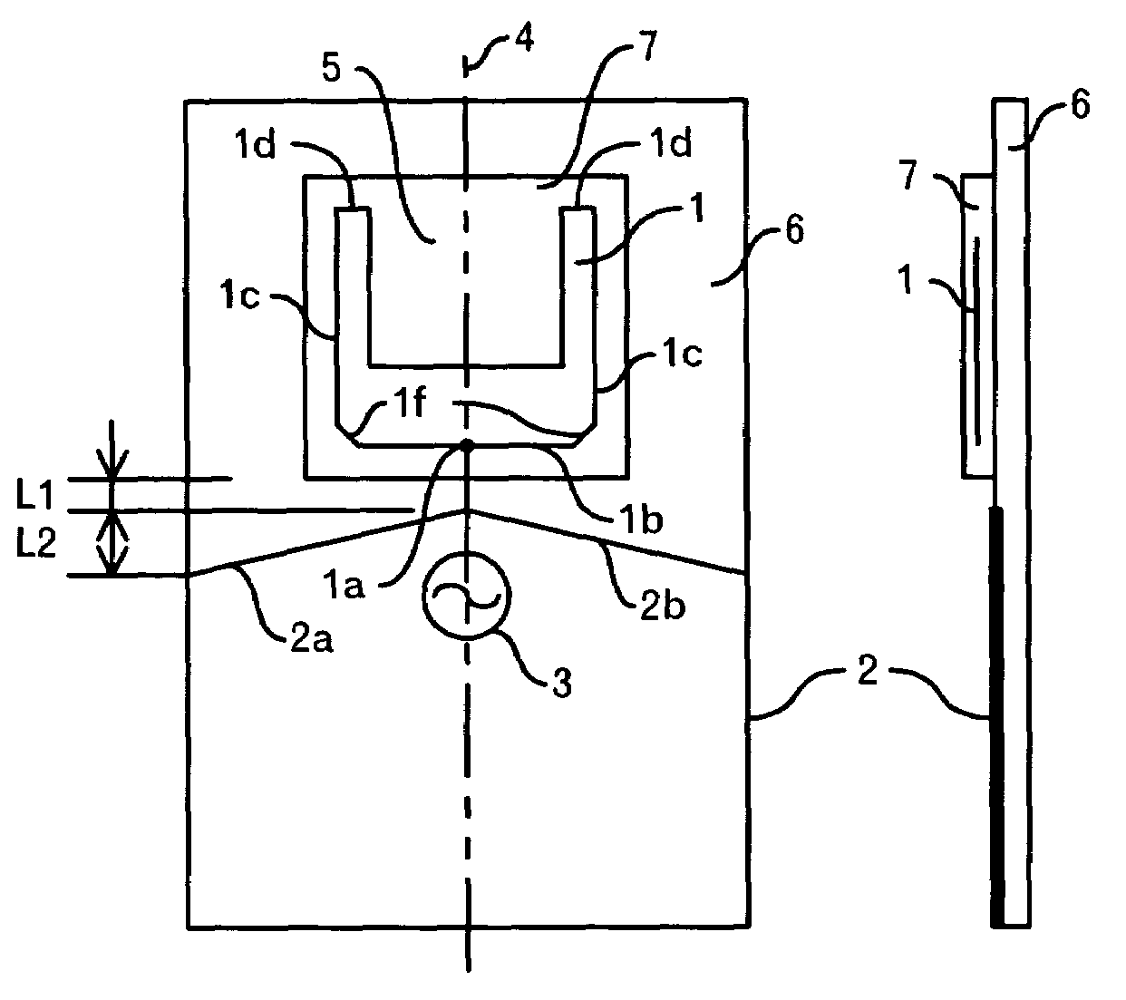
[0051]FIGS. 1A and 1B show the structure of an antenna according to a first embodiment of this invention. The antenna according to the first embodiment includes a dielectric substrate 7 that contains a conductive planar element 1 having a cut-out portion 5 therein and has a dielectric constant of about 20, a ground pattern 2 that is juxtaposed with the dielectric substrate 7 so as to make an interval of L1 (=1.0 mm) from the dielectric substrate 7 and in which a tapered shape is formed with respect to a feed point 1a of the planar element 1, a board 6, such as a printed circuit board (more specifically, a resin board made of FR-4, Teflon (registered trademark) or the like), and a high-frequency power source 3 connected to a feed point 1a of the planar element 1. The size of the dielectric substrate 7 is about 8 mm×10 mm×1 mm. In addition, the bottom side 1b of the planar element 1 is vertical to the line 4 passing through the feed point 1a, and the lateral sides 1...

second embodiment

2. Second Embodiment

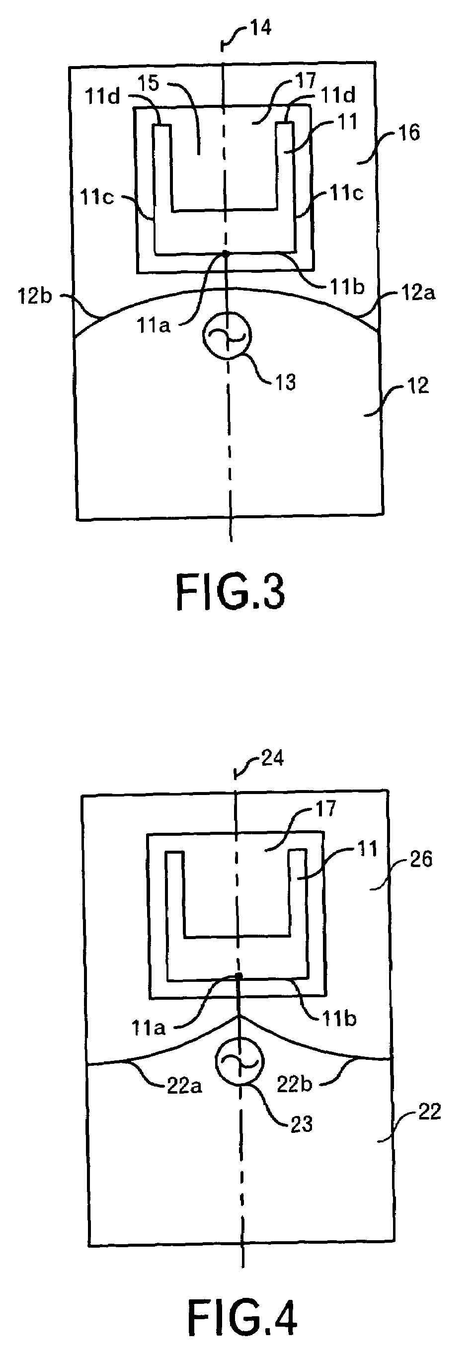
[0058]An antenna according to a second embodiment of the present invention comprises a dielectric substrate 17 that contains a planar element 11 therein and has a dielectric constant of about 20, a ground pattern 12 that is juxtaposed with the dielectric substrate 17 and has upper edge portions 12a and 12b that are upwardly convex curved lines, a board 16 such as a printed circuit board or the like, and a high-frequency power source 13 connected to a feed point 11a of the planar element 11 as shown in FIG. 3. The size of the dielectric substrate 17 is about 8 mm×10 mm×1 mm. In addition, the bottom side 11b of the planar element 11 is vertical to a line 14 passing through the feed point 11a, and lateral sides 11c connected to the bottom side 11b are parallel to the line 14. A cut-out portion 15 is provided at the top portion 11d of the planar element 11. The cut-out portion 15 is formed by concaving the top in a rectangular shape from the top portion 11d toward th...

third embodiment

3. Third Embodiment

[0062]As shown in FIG. 4, an antenna according to a third embodiment of the present invention comprises a dielectric substrate 17 containing a planar element 11 having the same shape as the second embodiment, a ground pattern 22 that is juxtaposed with the dielectric substrate 17 and has upper edge portions 22a and 22b which draw downward saturation curves, a board 26 such as a printed circuit board or the like on which the dielectric substrate 17 and the ground pattern 22 are mounted, and a high-frequency power source 23 connected to a feed point 11a of the planar element 11. The ground pattern 22 may be formed inside the board 26.

[0063]The planar element 11 and the ground pattern 12 are designed to be symmetric with respect to a line 24 passing through the feed point 11a. The length (hereinafter referred to as “distance”) of a line segment extending from any point on the bottom side 11b of the planar element 11 to the ground pattern 22 in parallel to the line 24...


PUM


Abstract

An antenna of this invention comprises an antenna element to which power is fed at a feed point; and a ground pattern that is juxtaposed with the antenna element and in which a tapered shape is formed with respect to the feed point of the antenna element. By providing the tapered shape for the ground pattern, it is possible to appropriately adjust the coupling degree with the antenna element, thereby it is possible to widen the bandwidth. Moreover, since the ground pattern and the antenna element are juxtaposed with each other, miniaturization can be achieved. When the antenna element is integrally formed in a dielectric substrate, further miniaturization can be achieved. Furthermore, when a cut-out portion is formed in the antenna element, the characteristic of the antenna in the low frequency range is improved.

Description

TECHNICAL FIELD OF THE INVENTION[0001]The present invention relates to a wide bandwidth antenna and a communication card using the wide bandwidth antenna.BACKGROUND OF THE INVENTION[0002]For example, JP-A-57-142003 discloses the following antennas. That is, it discloses a monopole antenna in which a flat-plate type radiation element 1001 having a disc shape is erected vertically to an earth plate or the ground 1002 as shown in FIGS. 16A-1 and 16A-2. This monopole antenna is designed so that a high-frequency power source 1004 and the radiation element 1001 are connected to each other through a power feeder 1003 and the height of the top portion of the radiation element 1001 is set to a quarter wavelength. Furthermore, it also discloses a monopole antenna in which a flat-plate type radiation element 1005 whose upper peripheral edge portion has a shape extending along a predetermined parabola is erected vertically to an earth plate or the ground 1002. Still furthermore, it discloses a ...

Claims


Application Information

Patent Timeline
Patent Type & Authority Patents(United States)
IPC IPC(8): H01Q1/38H01Q1/48H01Q13/08H01Q1/24H01Q9/28H01Q9/38H01Q9/40H01Q9/42
CPCH01Q1/38H01Q9/42H01Q9/285H01Q1/48
Inventor OKADO, HIRONORI
Owner TAIYO YUDEN KK
Why Eureka
Try Eureka