Touch pad of capacitive touch screen and manufacturing method thereof

A technology of capacitive touch screen and manufacturing method, applied in the direction of electric digital data processing, instrument, input/output process of data processing, etc., can solve problems such as large resistance difference, reduce resistance difference, improve touch accuracy and touch control performance, the effect of reducing the resistance

Inactive Publication Date: 2011-01-26
深圳市中显微电子有限公司
View PDF3 Cites 15 Cited by
  • Summary
  • Abstract
  • Description
  • Claims
  • Application Information

AI Technical Summary

Problems solved by technology

[0004] The purpose of the present invention is to provide a capacitive touch screen touch panel and its manufacturing method, to solve the technical defect that the X direction and Y direction resistance of the capacitive touch screen touch panel in the prior art are too different

Method used


Image

  • Touch pad of capacitive touch screen and manufacturing method thereof
  • Touch pad of capacitive touch screen and manufacturing method thereof
  • Touch pad of capacitive touch screen and manufacturing method thereof

Examples


no. 1 example

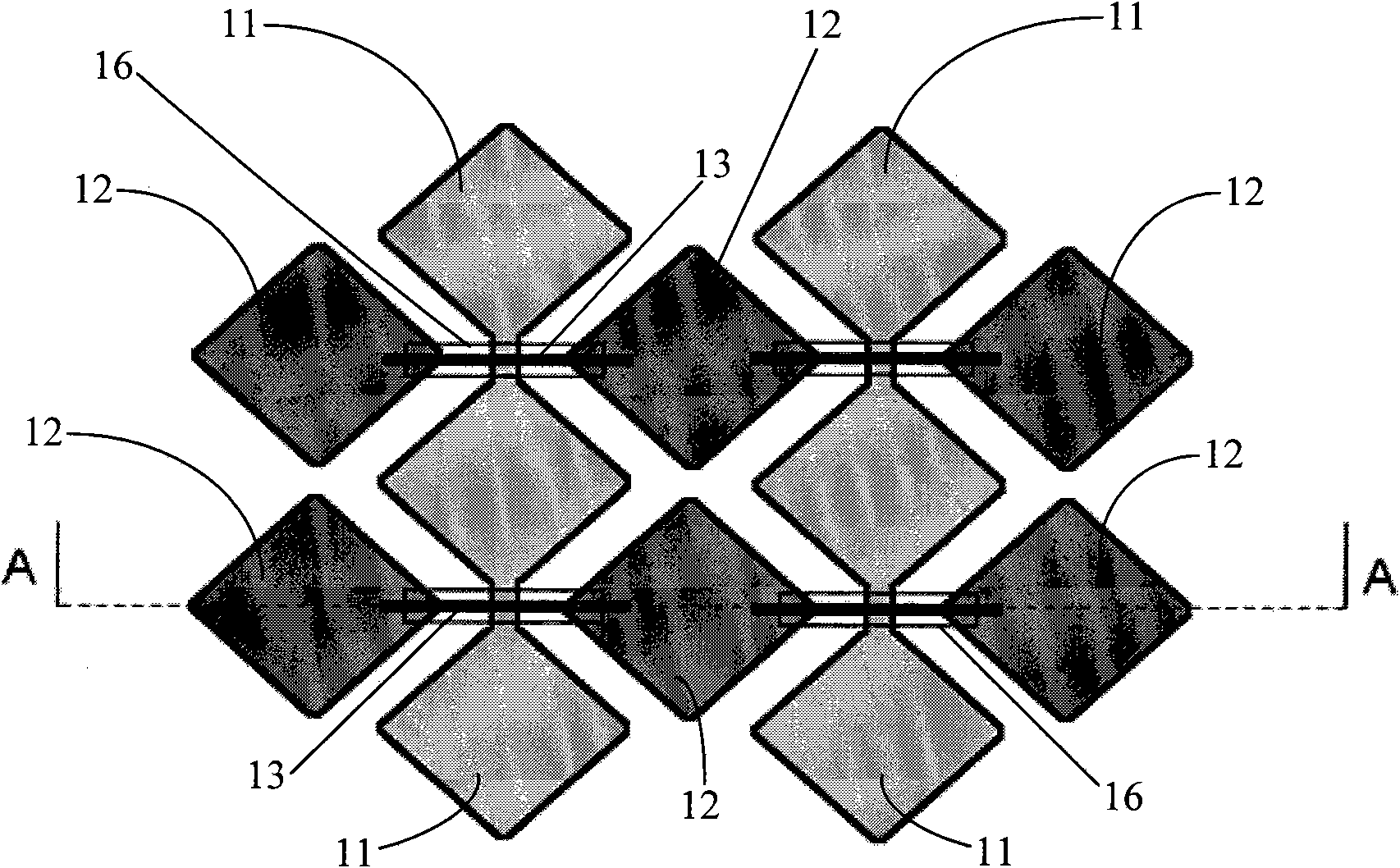
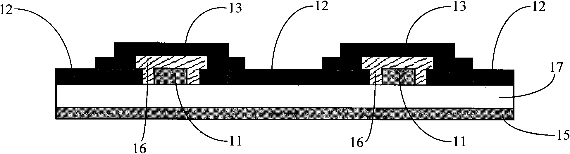
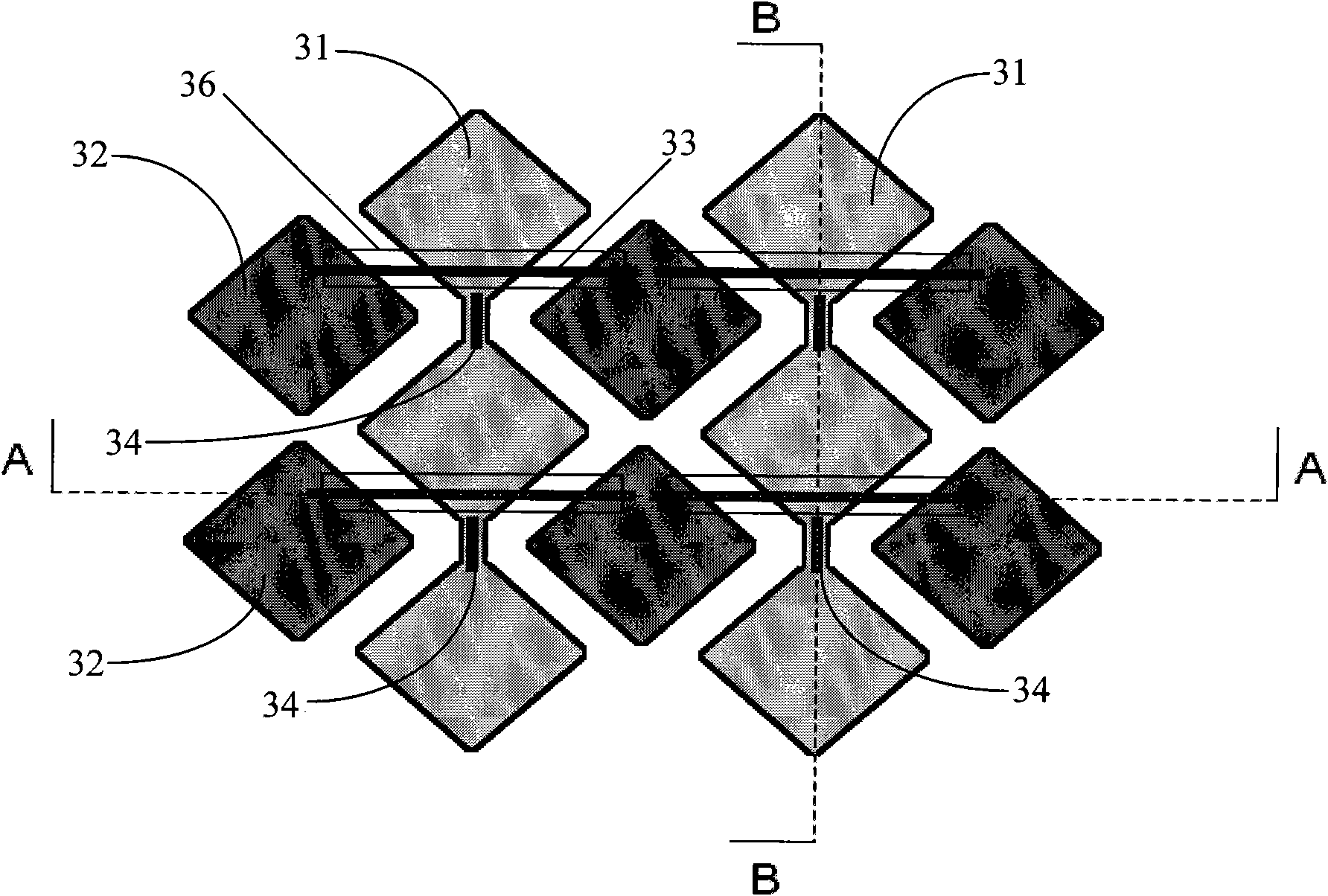
[0033] The first embodiment of the manufacturing method of the capacitive touch screen touch panel provided by the present invention comprises the following steps:

[0034] Step 41, coating one side of the substrate 37 with a transparent conductive film;

[0035] Step 42, photoetching the first layer of transparent conductive film, etching out the first group of conductive film lines 31 and the second group of conductive film lines 32, wherein the first group of conductive film lines 31 are continuous transparent conductive film lines, and the second group of conductive film lines The conductive film lines 32 are divided into sections by the first group of conductive film lines 31;

[0036] Step 43, coating a layer of insulating film on the first layer of transparent conductive film;

[0037] Step 44, photoetching out the insulating film line 36;

[0038] Step 45, plate a low-resistance conductive film on the first layer of transparent conductive film and the insulating film...


PUM


Abstract

The invention provides a touch pad of a capacitive touch screen and a manufacturing method thereof. The touch pad of the capacitive touch screen comprises a first group of conductive film lines and a second group of conductive film lines which are distributed on a substrate. Insulating film lines are arranged at intersections of the first and second groups of conductive film lines, wherein the upper surfaces of the insulating film lines are provided with a third group of conductive film lines which connects the second group of conductive film lines; and the narrowest part of the first group of conductive film lines is provided with a fourth group of conductive film lines. Compared with the prior art, the touch pad greatly reduces the resistance of the first group of conductive film lines by arranging the fourth group of conductive film lines on the narrowest part of the first group of conductive film lines, and greatly reduces the resistance of the second group of conductive film lines by adopting the third group of conductive film lines with low resistance to bridge the second group of conductive film lines. Therefore, the resistance of the first and second groups of conductive film lines is effectively reduced, a resistance difference between the first and second groups of conductive film lines is simultaneously reduced, and the touch performance of the touch screen is improved.

Description

technical field [0001] The invention relates to the field of touch screens, in particular to an improvement scheme for a touch panel of a capacitive touch screen. Background technique [0002] Such as figure 1 , figure 2 As shown in , the wiring of the touch panel of the existing capacitive touch screen is generally in the form of crossing the X direction (horizontal direction) and the Y direction (vertical direction), and the conductive film line 12 in the X direction and the conductive film line in the Y direction 11 is in the shape of a rhombus (or hexagon, etc.), in order to isolate the conductive film line 12 in the X direction and the conductive film line 11 in the Y direction, at the intersection of the conductive film lines 11 and 12, an insulation is provided between the two conductive film lines. Film line 16, like this, the conductive film line 12 of X direction is just divided into several sections by the conductive film line 11 of Y direction, then connects t...

Claims


Application Information

Patent Timeline
Patent Type & Authority Applications(China)
IPC IPC(8): G06F3/044
Inventor 姚伏恒
Owner 深圳市中显微电子有限公司
Why Eureka
Try Eureka