

Method for optimizing domain of CMOS (Complementary Metal-Oxide-Semiconductor) image sensor as well as etching method
- Summary
- Abstract
- Description
- Claims
- Application Information
AI Technical Summary
Problems solved by technology
Method used
Image

Examples
Embodiment Construction
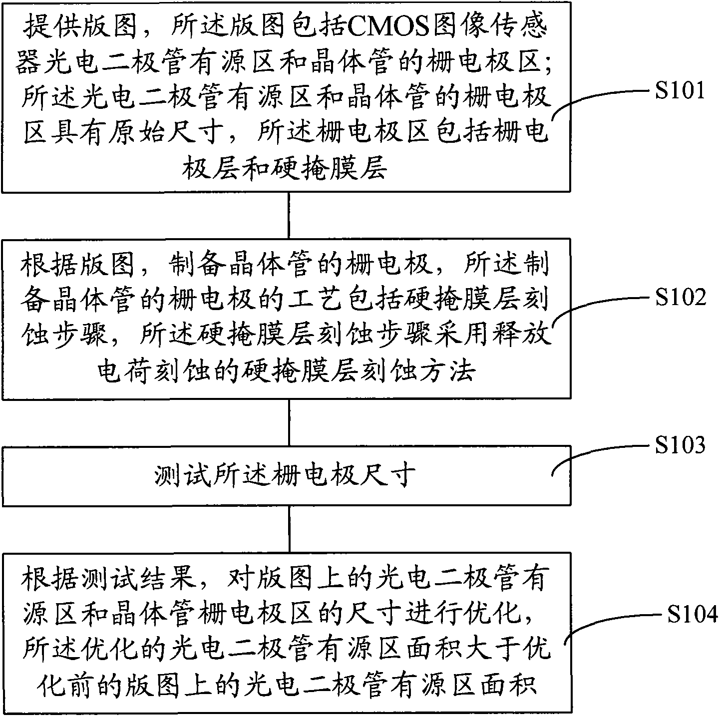
[0024] The present invention provides an embodiment of a method for optimizing the layout of a CMOS image sensor, such as image 3 shown, including the following steps:
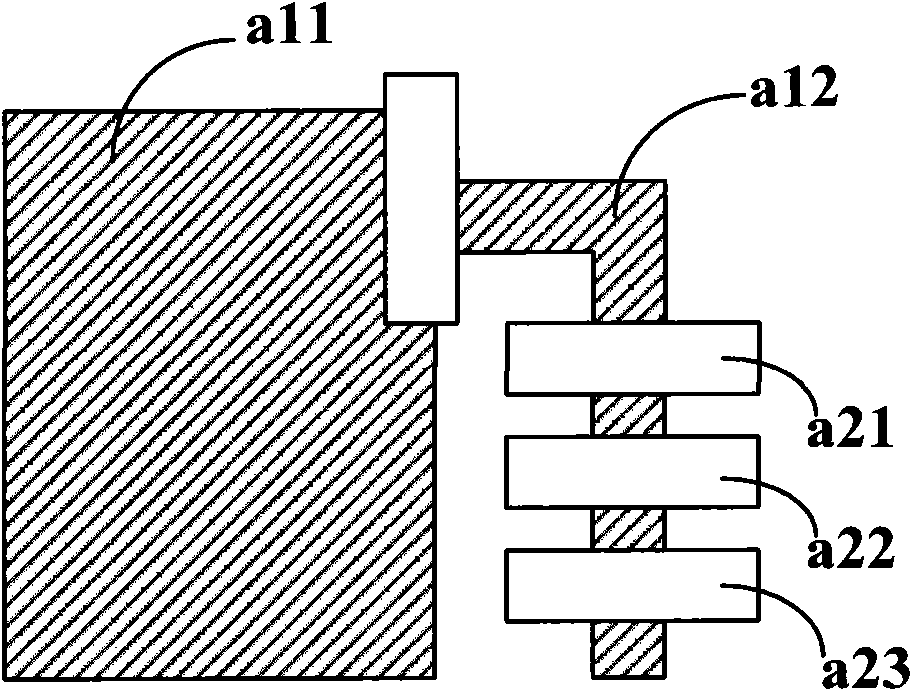
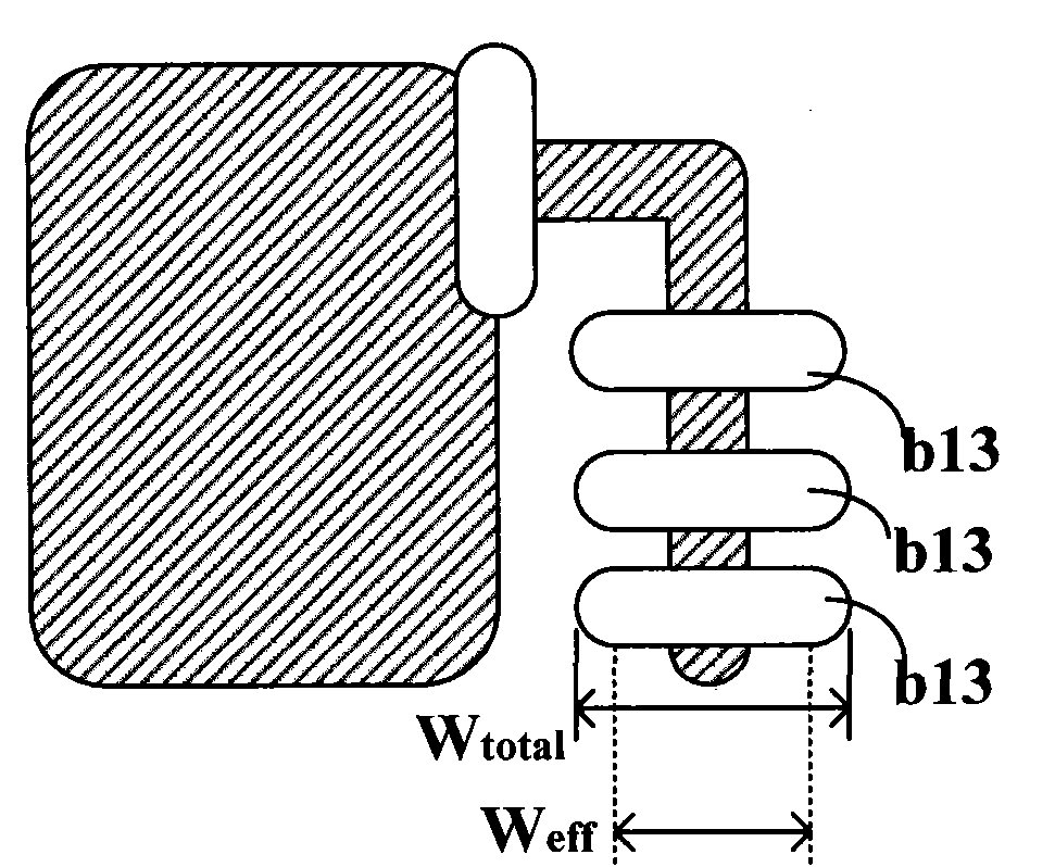
[0025] Step S101, providing a layout, the layout includes a CMOS image sensor photodiode active area and a gate electrode area of a transistor; the photodiode active area and the gate electrode area of a transistor have original dimensions, and the gate electrode area includes a gate electrode layer and hard mask layer;
[0026] Step S102, prepare the gate electrode of the transistor according to the layout, the process of preparing the gate electrode of the transistor includes a hard mask layer etching step, and the hard mask layer etching step adopts the hard mask layer etching of the release charge etching erosion method;
[0027] Step S103, testing the size of the gate electrode;
[0028] Step S104 , according to the test results, optimize the size of the photodiode active region and the gate elect...
PUM
 Abstract
Description
Claims
Application Information