Separation grid flash element and manufacture method thereof

A technology of split gate and manufacturing method, which is applied in semiconductor/solid-state device manufacturing, electrical components, electric solid-state devices, etc., and can solve problems affecting the yield and performance of split-gate flash components

Active Publication Date: 2008-06-11
TAIWAN SEMICON MFG CO LTD
View PDF5 Cites 0 Cited by
  • Summary
  • Abstract
  • Description
  • Claims
  • Application Information

AI Technical Summary

Problems solved by technology

After etching the conductive layer 40, trenches 100 will be formed in the unmasked active region 12, thereby affecting the yield and performance of split gate flash devices

Method used


Image

  • Separation grid flash element and manufacture method thereof
  • Separation grid flash element and manufacture method thereof
  • Separation grid flash element and manufacture method thereof

Examples


Embodiment Construction

[0038] Some of the following examples of the present invention will not describe well-known structures and processes to avoid unnecessary confusion. The preferred embodiments of the present invention will be described in detail below with accompanying drawings.

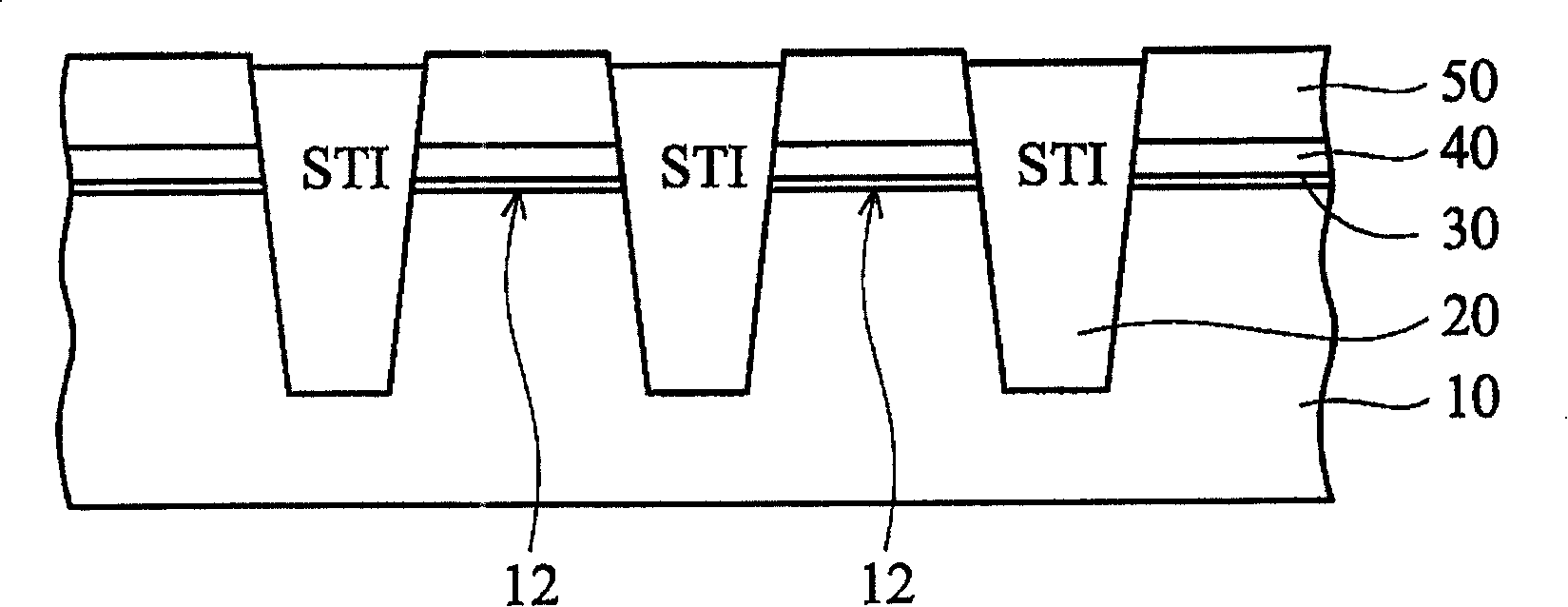
[0039] Figure 11 It is a cross-sectional view along the section line "2" in an embodiment of the present invention, and it is a split gate flash device before trenches are formed. Substrate 10 comprises any suitable semiconductor material or combination of materials, such as single crystal silicon or silicon-on-insulator (SOI). The dielectric layer 30 on the substrate 10 is a floating gate dielectric layer, which may include any dielectric material with a suitable dielectric constant and breakdown capacitance, preferably an oxide material, or silicon oxide thermally grown on the substrate 10 More preferably, the thickness is about 40 angstroms to 150 angstroms.

[0040] A conductive layer 40 is then formed on the ...


PUM


Abstract

A method for forming a split gate flash device is provided. In one embodiment, a semiconductor substrate with a dielectric layer formed thereover is provided. A conductor layer is formed overlying the dielectric layer. A masking layer is deposited overlying the conductor layer. A light sensitive layer is formed overlying the masking layer. The light sensitive layer is patterned and etched to form a pattern of openings therein. The masking layer and the conductor layer are etched according to the pattern of openings in the light sensitive layer. The conductor layer is etched at the outer surface area between the conductor layer and the dielectric layer to form undercuts. The dielectric layer is etched to form a notch profile at the outer surface area between the conductor layer and the dielectric layer and portions of the substrate are etched to form a plurality of trenches. An isolation layer is filled over the plurality of trenches and the masking layer. The masking layer and portions of the conductor layer and isolation layer are etched away, wherein a portion of the isolation layer is preserved in the notch profile.

Description

technical field [0001] The invention relates to a manufacturing method of a semiconductor memory element, in particular to a manufacturing method and structure of a split gate flash element. Background technique [0002] Split-gate flash memory devices are basically metal-oxide-semiconductor transistors with variable operating voltages. The operating voltage varies with the amount of charge stored in the floating gate structure. The floating gate structure is disposed on the first portion of the device channel region. A control gate structure is disposed on the second portion of the device's channel region. The control gate voltage regulated by the floating gate charge can directly control the second portion of the device channel region and indirectly control the first portion of the device channel region. The control gate is very close to the floating gate, so there will be capacitive coupling between the two. [0003] Over the years, flash memory has been significantly...

Claims


Application Information

Patent Timeline
Patent Type & Authority Patents(China)
IPC IPC(8): H01L21/8247H01L21/762H01L27/115
CPCH01L21/76224H01L27/11521H01L21/823481H01L27/115H10B69/00H10B41/30
Inventor 刘世昌罗际兴萧国裕蔡嘉雄
Owner TAIWAN SEMICON MFG CO LTD
Why Eureka
Try Eureka