Video processing circuit, video processing method, liquid crystal display apparatus, and electronic apparatus

一种图像处理、液晶分子的技术,应用在静态指示器、仪器等方向,能够解决开口率易降低、不能适用液晶面板、图像明亮限制等问题

Active Publication Date: 2011-04-06
SEIKO EPSON CORP
View PDF4 Cites 18 Cited by
  • Summary
  • Abstract
  • Description
  • Claims
  • Application Information

AI Technical Summary

Problems solved by technology

[0008] However, in the technology of reducing the reverse tilt domain by the structure of the liquid crystal panel, there is a disadvantage that the aperture ratio tends to decrease, and it cannot be applied to the already-made liquid crystal panel without improving the structure.
On the other hand, in the technique of removing image signals above the set value, there is a disadvantage that the brightness of the displayed image is limited by the set value.

Method used


Image

  • Video processing circuit, video processing method, liquid crystal display apparatus, and electronic apparatus
  • Video processing circuit, video processing method, liquid crystal display apparatus, and electronic apparatus
  • Video processing circuit, video processing method, liquid crystal display apparatus, and electronic apparatus

Examples


no. 1 Embodiment approach

[0040] Hereinafter, embodiments of the present invention will be described with reference to the drawings.

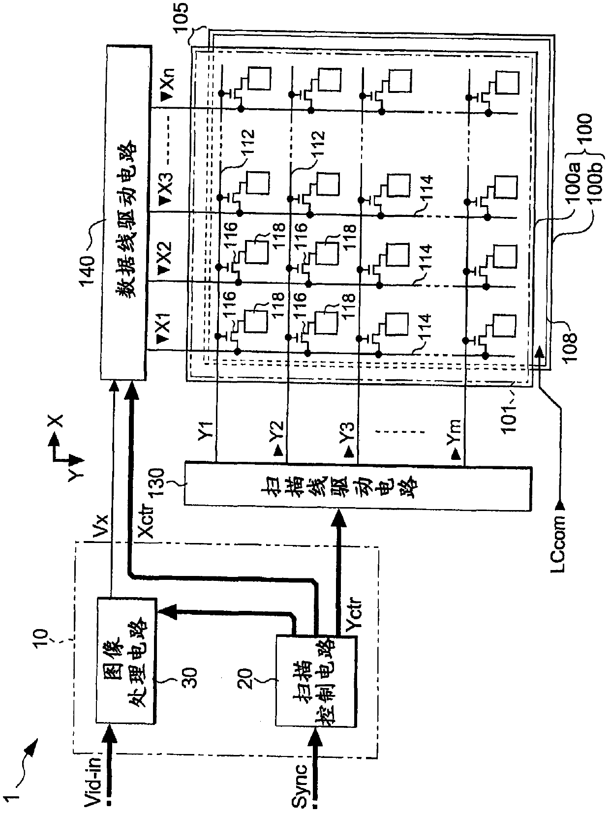
[0041] figure 1 It is a block diagram showing the overall configuration of a liquid crystal display device to which the image processing circuit according to this embodiment is applied.

[0042] As shown in the figure, the liquid crystal display device 1 includes a control circuit 10 , a liquid crystal panel 100 , a scanning line driving circuit 130 and a data line driving circuit 140 .

[0043]Among them, the image signal Vid-in is supplied to the control circuit 10 from the host device in synchronization with the synchronization signal Sync. The image signal Vid-in is digital data specifying the gradation level of each pixel of the liquid crystal panel 100, and is scanned according to a vertical scanning signal, a horizontal scanning signal, and a dot clock (both of which are omitted) included in the synchronization signal Sync. Available in order.

[0044] In addi...

no. 2 Embodiment approach

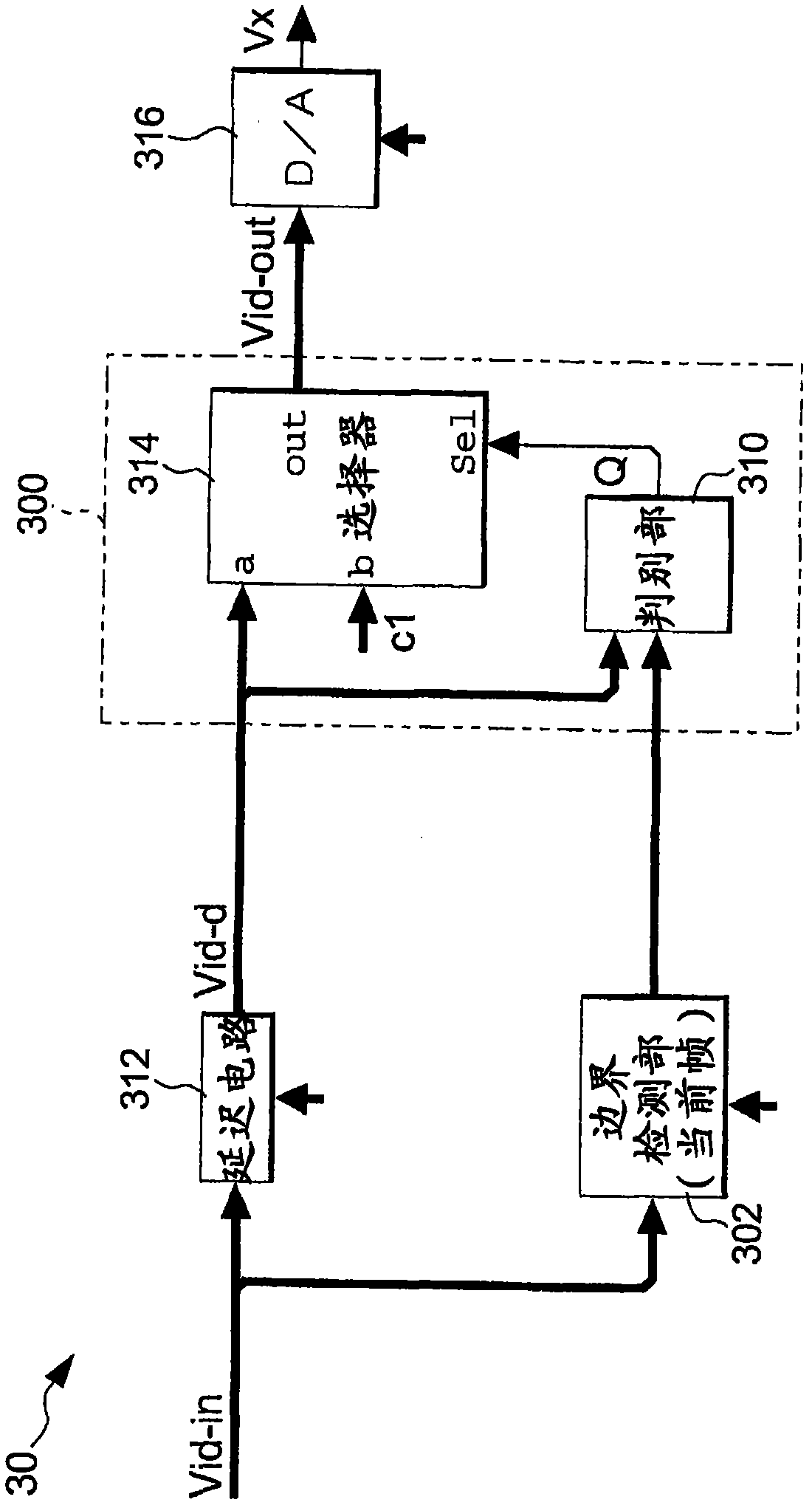
[0146] In the above-mentioned first embodiment, including the application / modification, the processing is completed in one frame of the image represented by the image signal Vid-in, but in the case of an image accompanied by motion, even in the In the frame (current frame) represented by the image signal Vid-in provided from the host device, pixels adjacent to the boundary may not need to be performed if the motion of a frame (previous frame) before the current frame is considered. fix.

[0147] Therefore, an image processing circuit according to the second embodiment that takes into account the state of the previous frame when correcting the current frame will be described next.

[0148] Figure 14 It is a block diagram showing the configuration of the image processing circuit according to the second embodiment.

[0149] exist Figure 14 in, with image 3 The composition shown is compared with the image 3 The configurations shown are different in that the application bo...


PUM


Abstract

The invention provides a video processing circuit, a processing method thereof, a liquid crystal display apparatus and an electronics device, which inhibit declination of display quality owing to influence of a horizontal electric field. A liquid crystal panel 100 has liquid crystal elements each including liquid crystals 105 interposed between the pixel electrode 118 arranged on an element substrate 100a and the common electrode 108 arranged on an opposite substrate. A video processing circuit 30, in a normally black mode, detects a frame of dark pixels of a liquid crystal element whose application voltage is smaller than a threshold Vth1 and bright pixels whose application voltage is larger or equal to the threshold Vth2, in correspondence with the gray scale designated by the image signal Vid-in and utilizes the application voltage of the dark pixels adjacent to the section of detected boundary change of a frame prior to the current frame to replace of the application corresponding to the gray level designated by the image signal of the current frame to a voltage Vc1 more than Vth1 and less than Vth2.

Description

technical field [0001] The present invention relates to a technique for reducing defects in display of a liquid crystal panel. Background technique [0002] A liquid crystal panel is a structure in which liquid crystal is sandwiched between a pair of substrates with a certain gap between them. [0003] In detail, the liquid crystal panel is configured such that pixel electrodes are arranged in a matrix for each pixel on one substrate, and common electrodes are common to pixels on the other substrate, and liquid crystal is sandwiched between the pixel electrodes and the common electrodes. When a voltage corresponding to the gray scale is applied and maintained between the pixel electrode and the common electrode, the alignment state of the liquid crystal is defined for each pixel, and thus the transmittance or reflectance is controlled. Therefore, in the above configuration, it can be said that among the electric fields acting on the liquid crystal molecules, only the direct...

Claims


Application Information

Patent Timeline
Patent Type & Authority Applications(China)
IPC IPC(8): G09G3/36G09G3/00G02F1/133
CPCG09G2320/0209G09G2320/0261G09G3/2011G09G3/3648G09G2320/103G09G3/36G09G2320/0233
Inventor 饭坂英仁保坂宏行
Owner SEIKO EPSON CORP
Why Eureka
Try Eureka