LED arrangement

A technology of LED devices and optical devices, applied in lighting devices, fixed lighting devices, components of lighting devices, etc., can solve the problem that LED packaging density is not optimal

Inactive Publication Date: 2011-04-20
SIEMENS AG
View PDF1 Cites 13 Cited by
  • Summary
  • Abstract
  • Description
  • Claims
  • Application Information

AI Technical Summary

Problems solved by technology

However, this has the disadvantage that, depending on the

Method used


Image

  • LED arrangement
  • LED arrangement
  • LED arrangement

Examples


Embodiment Construction

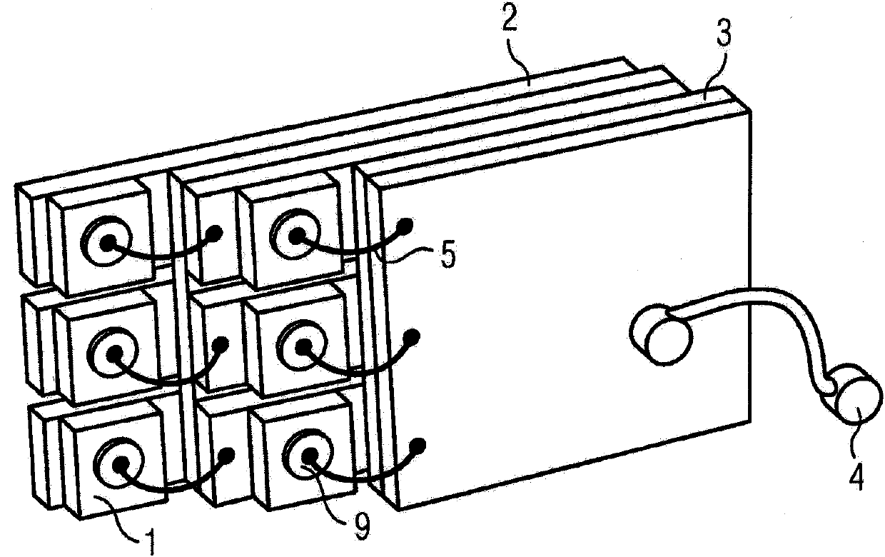
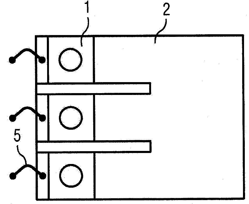
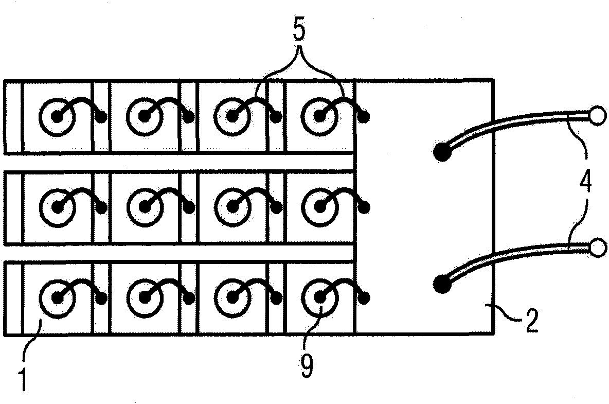
[0021] According to the invention, instead of mounting the light-emitting diodes (LEDs) on a common plane, a sandwich construction consisting of a plurality of metal films with interposed insulating layers is proposed. The key point is to use this structural method to achieve very dense placement of LED chips when viewed from the side. Furthermore, the heat generated during the operation of the LEDs can be dissipated from the LEDs respectively via the metal film.

[0022] This arrangement concept for realizing the carrier of the planar light emitter can also advantageously be designed with the following features:

[0023] To connect LEDs connected in series in different groups in parallel, as in figure 1 or figure 2 As illustrated in , the metal foil is formed, for example, in the form of a comb. In plan view, the trunk of the comb is provided with vertically extending comb teeth, wherein the multilayer films each extend to different extents up to the ends of the comb tee...


PUM


Abstract

LED arrangement (light emitting diode), comprising a plurality of adjacent radiating LEDs (1) that are nearly identically aligned for forming an extended area light source, wherein the LEDs are attached to a metallic multi-film support (2) comprising sandwich-like insulating intermediate layers (3) and having at least a step-like structure with at least one step, wherein at least one LED chip (1)is placed on each step on a metal film and the metal layer directly above comprises a corresponding shortening or recess for mounting an LED.

Description

technical field [0001] The invention relates to an arrangement of a plurality of LEDs (Light Emitting Diodes), which are mounted on a common support, emit light substantially in the same direction and thus form a planarly extending light source. Background technique [0002] In a structure based on an intense light source assembled from a plurality of light-emitting diodes (hereinafter referred to as LED chips or simply LEDs), a plurality of such elements are mounted on a common support. The contacting takes place outside of a common carrier, the individual elements being connected to each other. These methods work well for smaller devices in which eg 2x3 or 2xn LEDs are included. [0003] With the known planar two-dimensional arrangement of LEDs, intermediate spaces between the LEDs are presently provided for mounting a plurality of LEDs, as is exemplarily described according to US 2004 / 0233671 A1. [0004] The dense packing of light-emitting diodes planned according to t...

Claims


Application Information

Patent Timeline
IPC IPC(8): H01L25/075F21Y101/02
CPCH01L33/62H01L33/483H01L33/647H01L25/0753H01L2224/48227H01L33/486F21Y2107/50H01L2224/48091H01L2924/00014F21S8/04F21V19/00H01L25/075
Inventor 德特勒夫·格哈德
Owner SIEMENS AG
Why Eureka
Try Eureka