Hard substrate wafer sawing process

a technology of hard substrate wafers and sawing processes, which is applied in the direction of basic electric elements, electrical equipment, semiconductor devices, etc., can solve the problems of large area of dies (length by width) in contact with the adhesive surface of tape, sawing procedure appears to have reached a limit, and the rotation blade of the saw also produces vibrations

Active Publication Date: 2006-05-09
NORTHROP GRUMMAN SYST CORP
View PDF11 Cites 11 Cited by
  • Summary
  • Abstract
  • Description
  • Claims
  • Application Information

AI Technical Summary

Benefits of technology

[0016]In accordance with the foregoing objects and advantages, the sawing method enables small pieces of high aspect ratio to be sawed out from very hard materials while preventing the small pieces so produced from being scattered about by the coolant stream that cools the saw blade. As applied to the manufacture of semiconductor devices on sapphire, a very hard material, in this method a sapphire wafer containing semiconductor die is joined by thermoplastic material to a silicon carrier substrate, suitably a wafer of silicon, to form a unitary sandwich assembly in preparation for sawing out the die from the wafer. The thermoplastic produces a bond strong enough to hold the die in place against the shear force exerted on the die by the stream of liquid coolant used to cool the saw blade during sawing and by the rotating saw blade as the saw cuts through the sapphire wafer, even when the die are of a high aspect ratio. Afterwards, the thermoplastic material is chemically removed and the die may be picked individually from the silicon carrier substrate.

Problems solved by technology

The rotating blade of the saw also produces vibrations.
The adhesive tape prevents the die that are cut from the wafer from being blasted away by the force of the coolant water stream during the sawing procedure or bounced off the wafer support by the vibration, both of which are undesirable.
However, in those previous applications, the area of the die (length by width) in contact with the adhesive surface of the tape is relatively large.
That convenient and widely employed sawing procedure appears to have reached a limit with the advance in transistor technology.
Quite routinely, the described sawing procedure was applied to the manufacture of the Gallium Nitride transistor, but with devastating effect.
Of the two appropriate substrate materials for the GaN, Silicon carbide is prohibitively expensive, leaving sapphire as the substrate of economic choice for the GaN transistors.
That coolant flow produced two profound adverse effects.
First, localized heating from the interaction of the saw blade with the hard material led to a breakdown in the adhesive properties of the adhesive tape.
Secondly, the increased coolant flow produced sufficient force to detach and blow the individual die formed by the sawing from the tape, scattering the die about.
The scattered die were thus considered contaminated and could not be used.
The tried and true prior art sawing process failed.
Lessening the coolant flow rate was not a practical alternative, since frequent replacement of the saw blades alone was too expensive.
Increasing the strength of the adhesive was also not a solution.
The adhesive strength would have to be increased so greatly as would make it difficult or impossible to pluck die from the tape on completion of sawing.
However, the number of die that could be fabricated on a given wafer would be reduced by three-quarters, prohibitively increasing the cost of a chip and rendering the chip economically unfeasible.

Method used


Image

  • Hard substrate wafer sawing process
  • Hard substrate wafer sawing process
  • Hard substrate wafer sawing process

Examples


Embodiment Construction

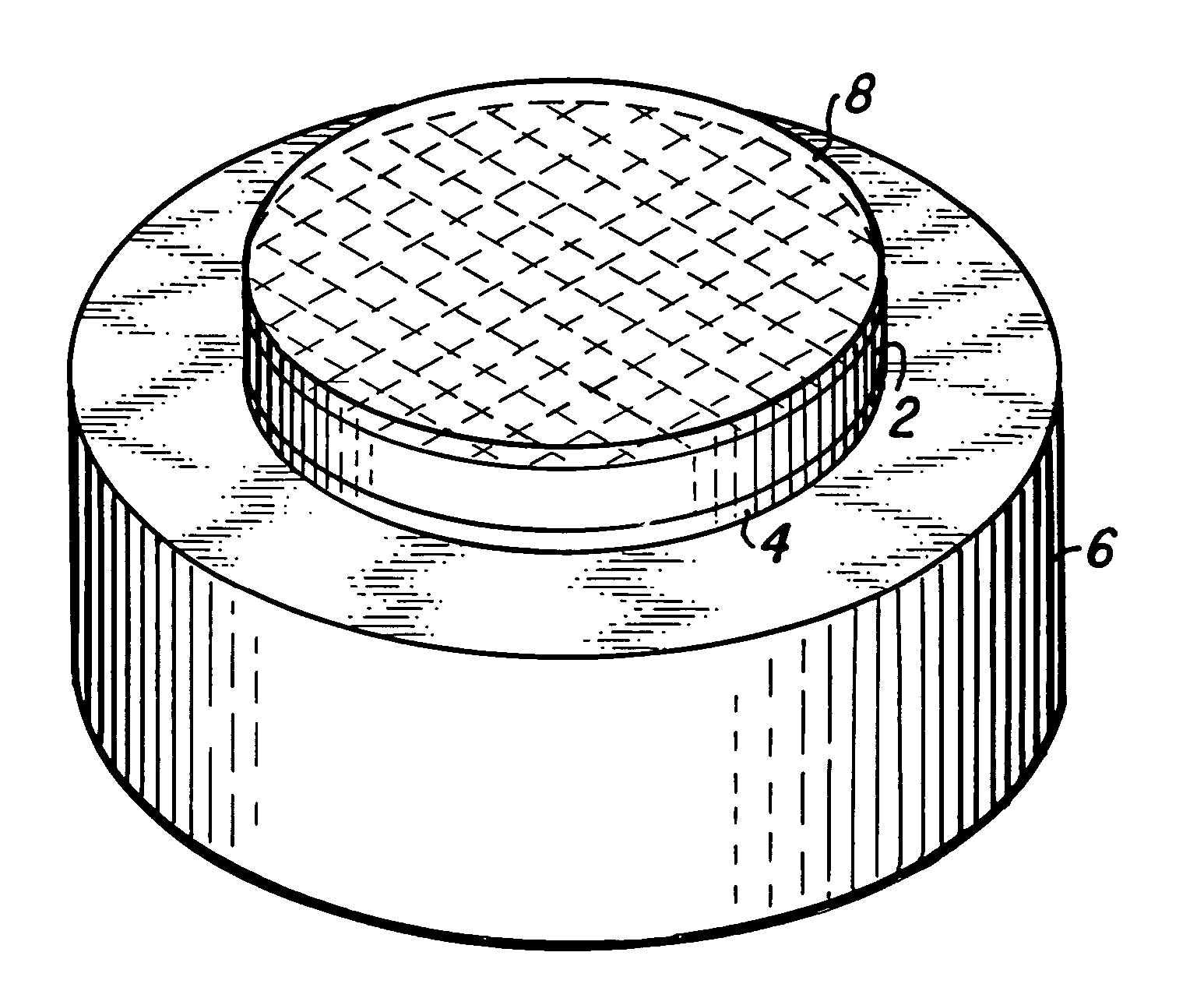
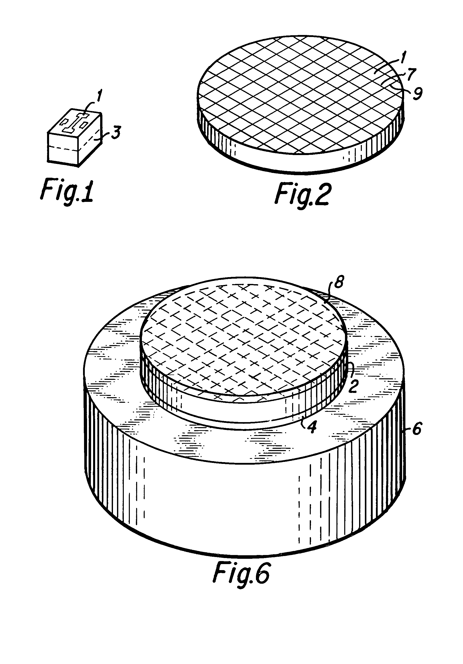
[0027]Sawing of a semiconductor wafer is accomplished after the wafer has been processed to form a large number of copies of a semiconductor device on the upper surface, such as the semiconductor device 1 pictorially illustrated (not-to-scale) in the die or chip 3 in FIG. 1. As pictorially represented in FIG. 2, those semiconductor devices 1, only one of which is numbered, are typically arranged in a regular grid-like pattern on the surface of the wafer 2, spaced a short distance from one another in rows and columns. That arrangement enables a circular saw to be moved along a series of parallel lines, the saw lines, first in one direction 7, and then in an orthogonal direction 9 thereto to define the small separate square or rectangular shaped regions of wafer real estate, referred to as chips or die.

[0028]Typically, the formed semiconductor devices extend a short distance into the depth of the processed wafer. The remainder of the wafer thickness or height constitutes solely the su...


PUM


Abstract

Die of high aspect ratio formed in a hard wafer substrate are sawed out without requiring tape, obtaining high die yields. Preliminary to sawing the semiconductor die (3) from a sapphire wafer (2), the wafer is joined (20) to a silicon carrier substrate (6) by a thermoplastic layer (4) forming a unitary sandwich-like assembly. Sawing the die from the wafer follows. The thermoplastic is removed, and the die may be removed individually (50) from the silicon carrier substrate. Thermoplastic produces a bond that holds the die in place against the shear force exerted by the saw and by the stream of coolant (30).

Description

FIELD OF THE INVENTION[0001]This invention relates to the manufacture of semiconductor chips and, more particularly, to the process of sawing semiconductor chips that possess a large aspect ratio from the wafer substrate, where the substrate is a very hard material.BACKGROUND[0002]A conventional procedure for manufacture of semiconductor chips in commercial quantities is to fabricate or process a great number, hundreds or thousands, of identical chips simultaneously on a large size wafer of substrate material. Each semiconductor chip defines or contains a copy of the circuit of a power amplifier, low noise amplifier, computer processor, an electronic component or electronics components of greater complexity. That circuit fabrication on the wafer typically uses conventional doping, photoresist and etching processes, the details of which are well known and not relevant to the present invention. Once circuit fabrication is completed, the wafer is cut apart, parsed, into individual chip...

Claims


Application Information

Patent Timeline
Patent Type & Authority Patents(United States)
IPC IPC(8): H01L21/301H01L21/46H01L21/68H01L21/78
CPCH01L21/6836H01L21/78H01L2221/68327
Inventor BARSKY, MICHAEL EDWARDWOJTOWICZ, MICHAELSANDHU, RAJINDER RANDY
Owner NORTHROP GRUMMAN SYST CORP
Why Eureka
Try Eureka