LED package and method for manufacturing the same

A technology of LED packaging and LED chips, applied in semiconductor devices, electrical components, circuits, etc., can solve problems such as easy degradation of resin

Inactive Publication Date: 2011-08-03
KK TOSHIBA
View PDF4 Cites 10 Cited by
  • Summary
  • Abstract
  • Description
  • Claims
  • Application Information

AI Technical Summary

Problems solved by technology

Meanwhile, the resin portion sealing the LED chip is easily deteriorated due to the increase of light and heat radiated from the LED chip

Method used


Image

  • LED package and method for manufacturing the same
  • LED package and method for manufacturing the same
  • LED package and method for manufacturing the same

Examples


Embodiment Construction

[0024] Hereinafter, embodiments of the present invention will be described with reference to the drawings.

[0025] First, the first embodiment is described.

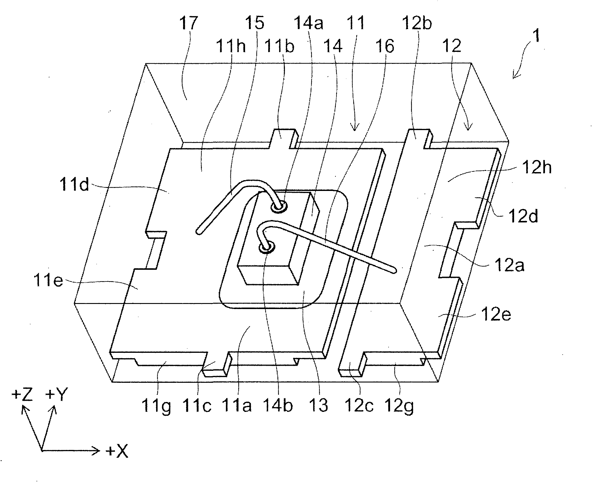
[0026] figure 1 is a perspective view illustrating the LED package according to the present embodiment.

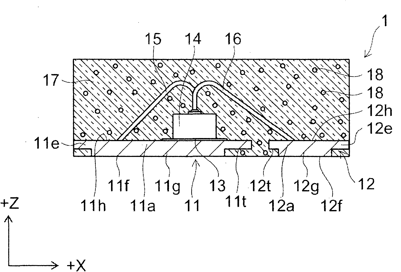
[0027] Figure 2A is a sectional view illustrating the LED package according to the present embodiment. Figure 2B is a plan view illustrating an example lead frame.

[0028] like Figures 1 to 2B As shown, the LED package 1 according to this embodiment includes a pair of lead frames 11 and 12 . The lead frames 11 and 12 each have a flat shape and are arranged separately from each other on the same plane. The lead frames 11 and 12 are formed of the same metal material. Note that examples of the metal material include pure metals and alloys. The lead frames 11 and 12 may be formed of various metal materials. For example, each of the lead frames 11 and 12 may include a metal plate made of a specific metal mat...


PUM


Abstract

The present invention provides an LED package and a method for manufacturing the same. According to one embodiment, the LED package includes first and second lead frames, an LED chip and a resin body. The first and second lead frames are made of a metal material, and disposed to be apart from each other. The LED chip is provided above the first and second lead frames, the LED chip having one terminal connected to the first lead frame and another terminal connected to the second lead frame. The resin body is made of a resin material having a shore D hardness of 25 or higher. In addition, the resin body covers the first and second lead frames and the LED chip. And, an appearance of the resin body is an appearance of the LED package.

Description

[0001] Cross References to Related Applications [0002] This application is based on and claims priority from prior Japanese Patent Application No. 2010-019769 filed on January 29, 2010, the entire contents of which are hereby incorporated by reference. technical field [0003] Embodiments described herein generally relate to LED packages and methods of manufacturing the same. Background technique [0004] Conventionally, an LED package mounted with an LED chip is configured in such a manner as to control light distribution characteristics and improve light extraction efficiency from the LED package. Specifically, the LED package is provided with a cup-shaped case made of white resin. Then, LED chips are mounted on the bottom surface of the case. The inside of the case is filled with a transparent resin to bury the LED chip therein. In many cases, the housing is formed of thermoplastic polyamide resin (see, for example, Japanese Patent Application Publication No. JP-A 20...

Claims


Application Information

Patent Timeline
Patent Type & Authority Applications(China)
IPC IPC(8): H01L33/48H01L33/62H01L33/56
CPCH01L33/48H01L2224/48247H01L33/62H01L2924/01322H01L24/97H01L2224/48091H01L2224/32245H01L2924/12041H01L33/56H01L2224/73265H01L2224/48465H01L2224/97H01L2924/351H01L2924/181H01L2924/12035H01L2924/00014H01L2924/00012H01L2924/00
Inventor 渡元清水聪押尾博明刀祢馆达郎岩下和久小松哲郎竹内辉雄
Owner KK TOSHIBA
Why Eureka
Try Eureka