Semiconductor device and method of manufacturing the same

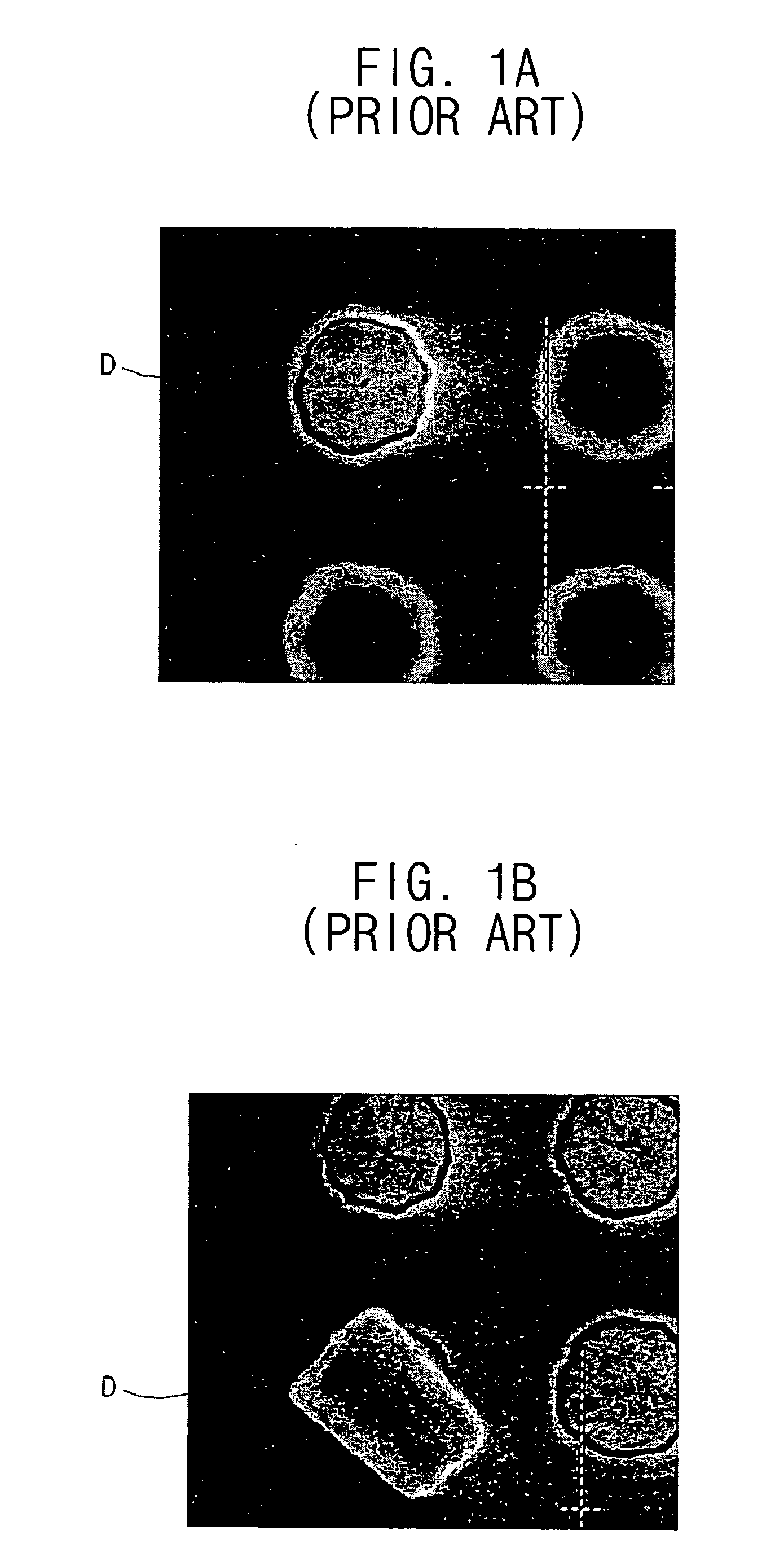
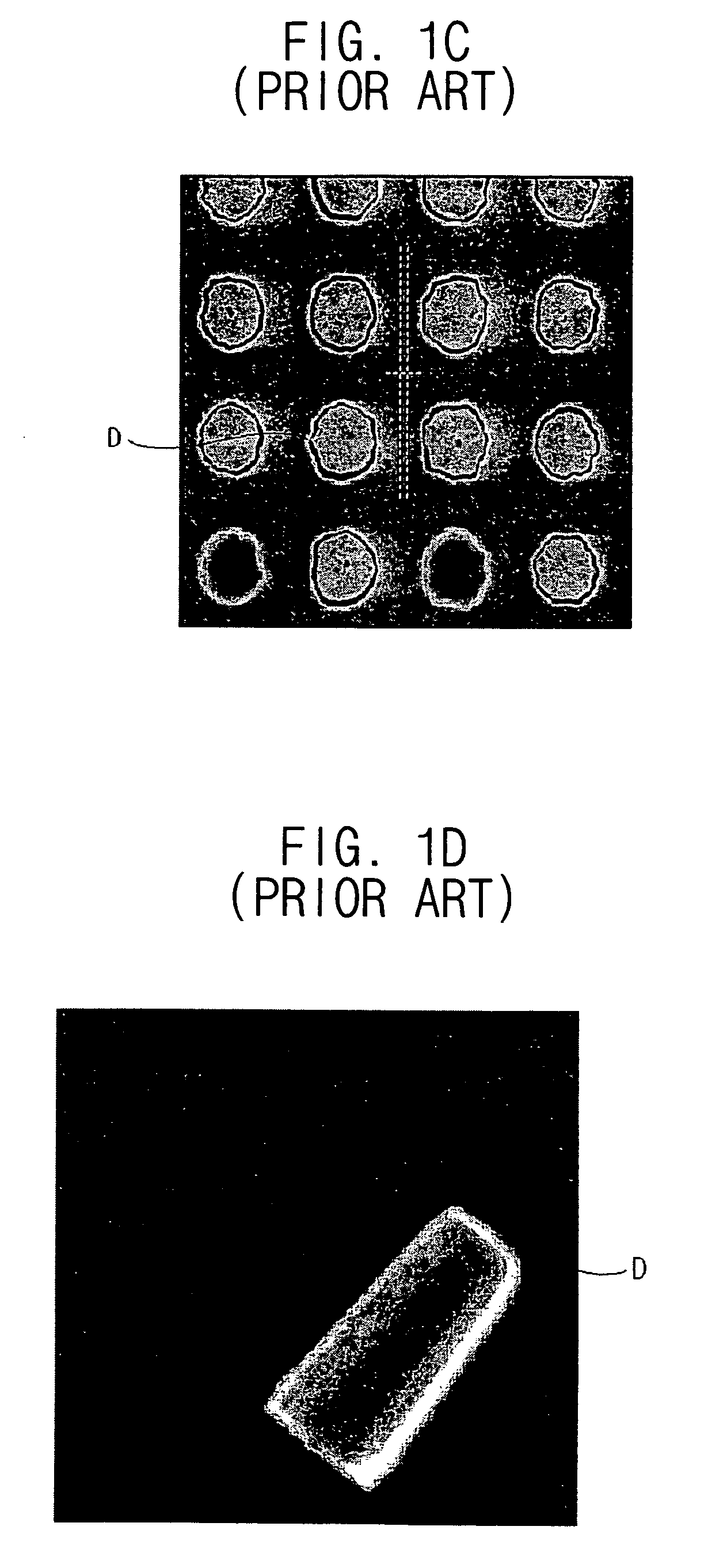
a technology of semiconductor devices and semiconductors, applied in semiconductor devices, semiconductor/solid-state device details, electrical apparatus, etc., can solve the problems of damage to the inner surface of the contact hole or the via hole, rapid increase of the aspect ratio of the contact hole, and filling up

Active Publication Date: 2009-01-15
SAMSUNG ELECTRONICS CO LTD
View PDF3 Cites 201 Cited by
  • Summary
  • Abstract
  • Description
  • Claims
  • Application Information

AI Technical Summary

Benefits of technology

[0018]According to the present invention there is provided a method of manufacturing a semiconductor device for preventing a barrier layer of a metal wiring structure from being removed from an insulation layer at an upper portion of a contact hole in a planarization process for forming a plug of the metal wiring.

Problems solved by technology

Particularly, the small widths of the metal wiring can cause a rapid increase of an aspect ratio of a contact hole or a via hole, and thus there are difficulties in filling up the contact hole or the via hole by a conventional deposition process.
However, tungsten has many disadvantages in a formation process of the plug or the wiring in that a tungsten layer can have difficulty in adhering to an oxide layer and source gases in a deposition process for the plug or the wiring can cause damage to the inner surface of the contact hole or the via hole.
However, the above conventional process for forming the contact plug and the metal wiring has a problem in that the first tungsten layer is removed from the insulation interlayer simultaneously with the second tungsten layer in the planarization process.
Therefore, there is a problem in that the contact hole or the via hole may not be sufficiently filled with the plug and the plug may be spaced apart from the inner surface of the hole by a distance.
Particularly, when the first tungsten layer is removed from a bottom of the contact hole or the via hole at which the plug structure makes contact with the silicon substrate, the contact resistance between the silicon substrate and the contact plug can be significantly increased, thereby causing electrical shorts and device failures.

Method used


Image

  • Semiconductor device and method of manufacturing the same
  • Semiconductor device and method of manufacturing the same
  • Semiconductor device and method of manufacturing the same

Examples


Embodiment Construction

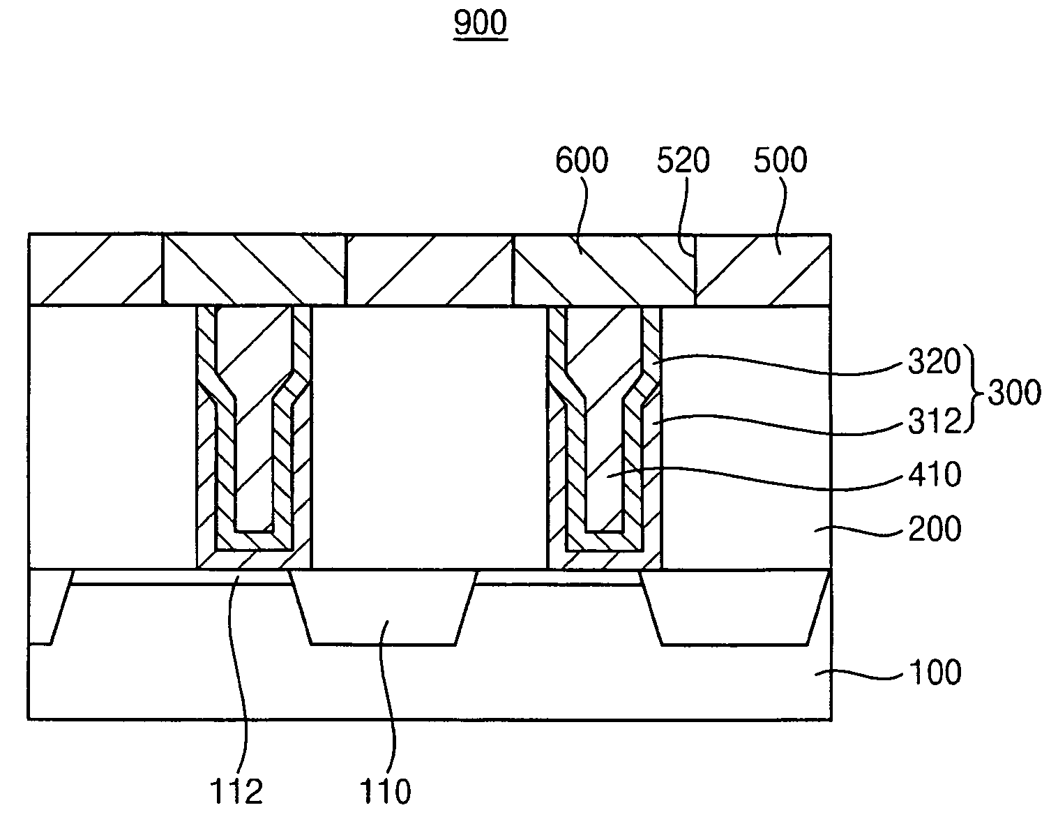
[0055]Embodiments in accordance with aspects of the present invention are described more fully hereinafter with reference to the accompanying drawings. This invention can, however, be embodied in many different forms and should not be construed as limited to the embodiments set forth herein. In the drawings, the size and relative sizes of layers and regions may be exaggerated for clarity.

[0056]It will be understood that when an element or layer is referred to as being “on,”“connected to” or “coupled to” another element or layer, it can be directly on, connected or coupled to the other element or layer or intervening elements or layers can be present. In contrast, when an element is referred to as being “directly on,”“directly connected to” or “directly coupled to” another element or layer, there are no intervening elements or layers present. Like numbers refer to like elements throughout. As used herein, the term “and / or” includes any and all combinations of one or more of the assoc...


PUM

PropertyMeasurementUnit
internal pressureaaaaaaaaaa
bias poweraaaaaaaaaa
temperatureaaaaaaaaaa

Abstract

In a method of forming a wiring structure for a semiconductor device, an insulation layer is formed on a semiconductor substrate on which a plurality of conductive structures is positioned. An upper surface of the insulation layer is planarized and spaces between the conductive structures are filled with the insulation layer. The insulation layer is partially removed from the substrate to form at least one opening through which the substrate is partially exposed. A residual metal layer is formed on a bottom and a lower portion of the sidewall of the at least one opening and a metal nitride layer is formed on the residual metal layer and an upper sidewall of the opening with a metal material. Accordingly, an upper portion of the barrier layer can be prevented from being removed in a planarization process for forming the metal plug.

Description

CROSS-REFERENCE TO RELATED APPLICATIONS[0001]This application claims priority under 35 U.S.C. §119 to Korean Patent Application No. 10-2007-0069887, filed on Jul. 12, 2007 in the Korean Intellectual Property Office (KIPO), the contents of which are herein incorporated by reference in their entirety.BACKGROUND OF THE INVENTION[0002]1. Field of the Invention[0003]The present invention relates to a semiconductor device and a method of manufacturing the same, and more particularly, to a method of manufacturing a semiconductor device in which a barrier layer of a wiring structure has improved adhesion to an insulation layer, and a semiconductor device manufactured by the same method.[0004]2. Description of the Related Art[0005]Nowadays, as semiconductor devices are becoming highly integrated, sizes of source / drain regions and widths of gate electrodes and metal wiring in semiconductor 20 devices are being rapidly reduced. Particularly, the small widths of the metal wiring can cause a rap...

Claims


Application Information

Patent Timeline
Patent Type & Authority Applications(United States)
IPC IPC(8): H01L21/768H01L23/532
CPCH01L21/28562H01L21/76846H01L21/76865H01L23/485H01L2924/0002H01L27/10891H01L2924/00H10B12/488H01L21/28
Inventor PARK, JIN-HOCHOI, GIL-HEYUNLEE, SANG-WOOLEE, HO-KI
Owner SAMSUNG ELECTRONICS CO LTD
Why Eureka
Try Eureka