Non-volatile memory devices and methods of operating the same
What is Al technical title?
Al technical title is built by PatSnap Al team. It summarizes the technical point description of the patent document.
a memory device and non-volatile technology, applied in semiconductor devices, instruments, electrical devices, etc., can solve the problems of increasing the operating voltage of the memory device, increasing the complexity of the associated peripheral circuitry, and it is more difficult to provide high integration density and low power consumption for floating gate type memory devices than for floating trap type memory devices
Inactive Publication Date: 2006-08-17
SAMSUNG ELECTRONICS CO LTD
View PDF66 Cites 177 Cited by
Summary
Abstract
Description
Claims
Application Information
AI Technical Summary
This helps you quickly interpret patents by identifying the three key elements:
Problems solved by technology
Method used
Benefits of technology
Problems solved by technology
A thicker tunneling insulating layer may result in an increased operating voltage for the memory device and an increased complexity of associated peripheral circuitry.
Consequently, it may be more difficult to provide high integration density and low power consumption for floating gate type memory devices than for floating trap type memory devices.
Differences between the energy band gaps may result in potential barriers at the interfaces between the materials.
The thickness of the silicon oxide layer may affect the data retention tim
Method used
Image
Click on the blue label to locate the original text in one second.
Reading with bidirectional positioning of images and text.
Examples
Embodiment Construction
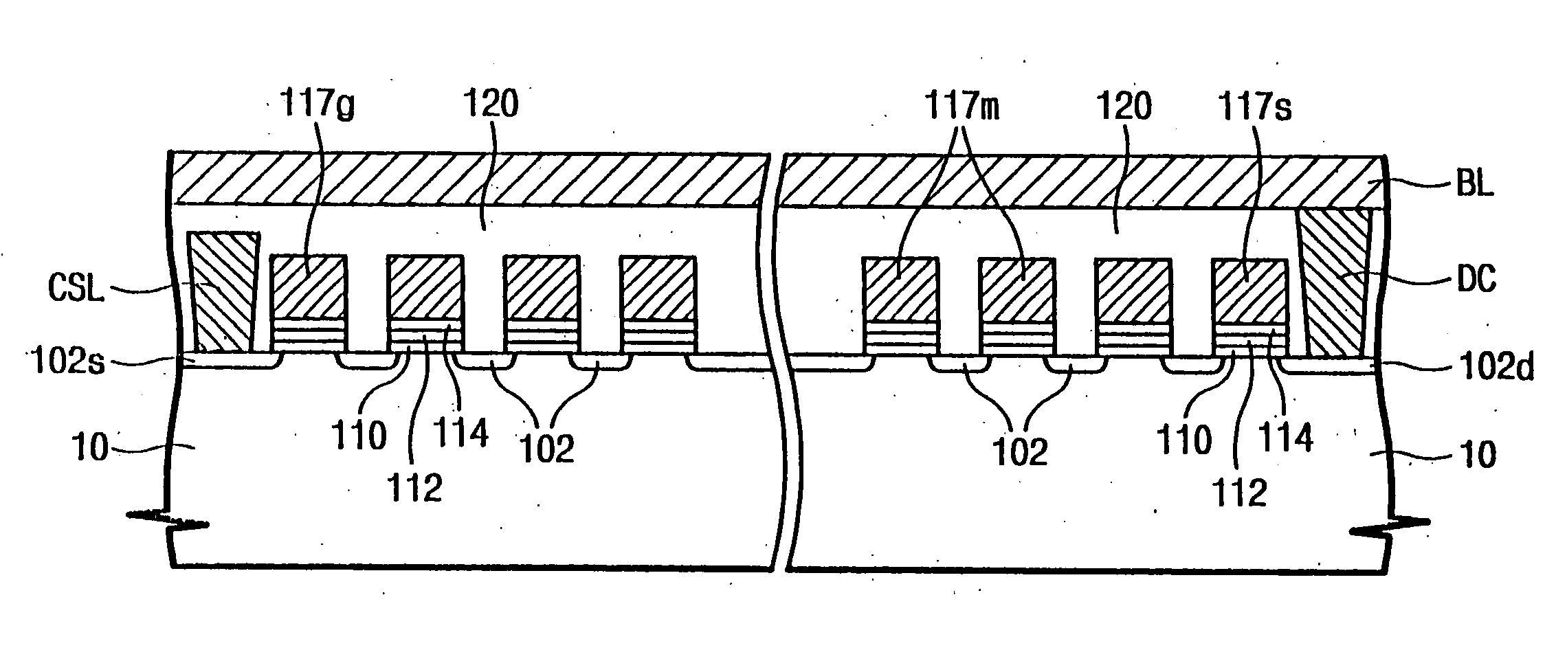
[0045] The present invention will now be described more fully with reference to the accompanying drawings, in which preferred embodiments of the invention are shown. This invention may, however, be embodied in many different forms and should not be construed as being limited to the embodiments set forth herein. Rather, these embodiments are provided so that this disclosure will be thorough and complete, and will fully convey the concept of the invention to those skilled in the art. In the drawings, the thickness of layers and regions are exaggerated for clarity. It will also be understood that when a layer is referred to as being “on” another layer or substrate, it can be directly on the other layer or substrate, or intervening layers may also be present. In contrast, when an element is referred to as being “directly on” another element, there are no intervening elements present.
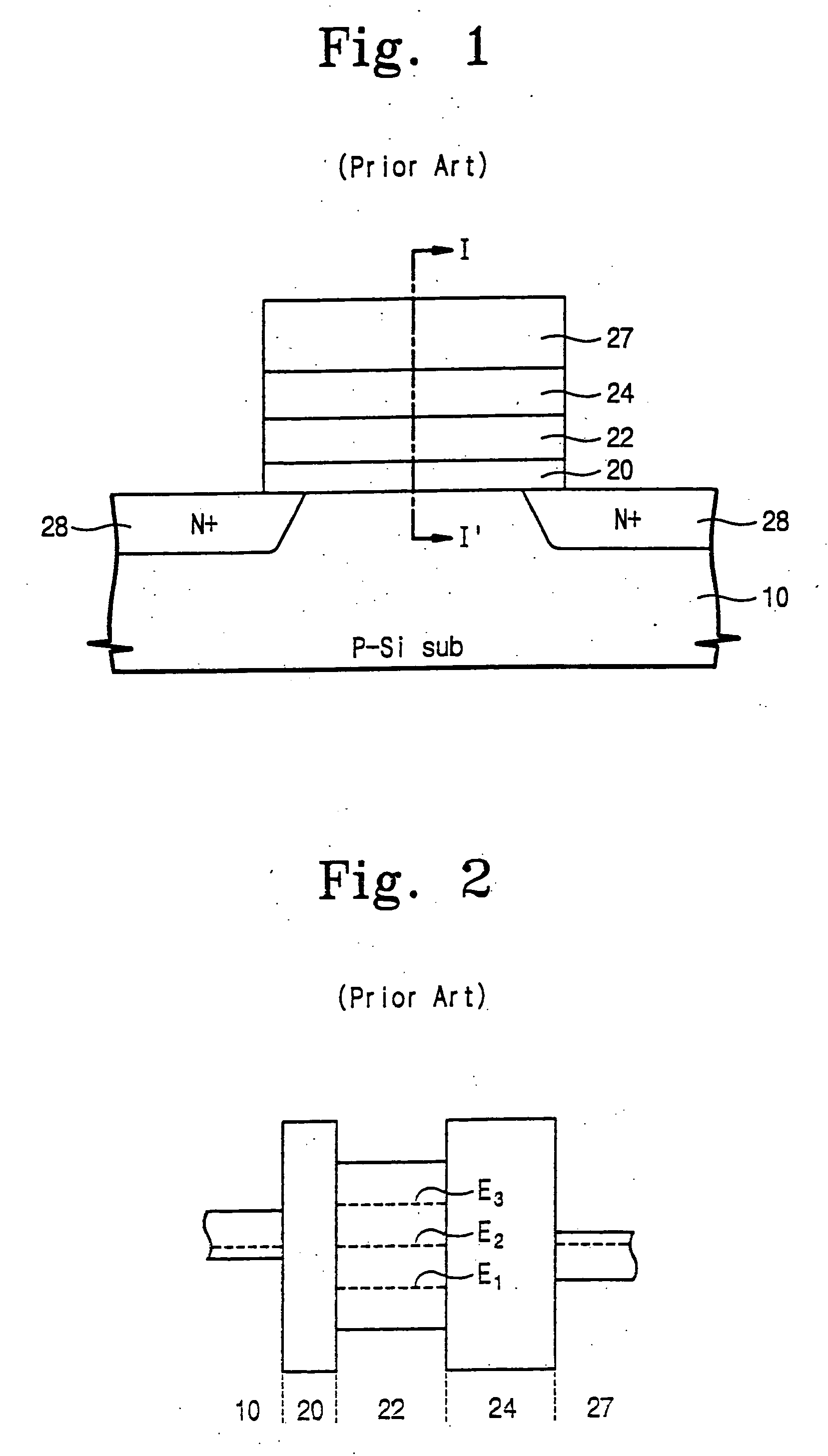
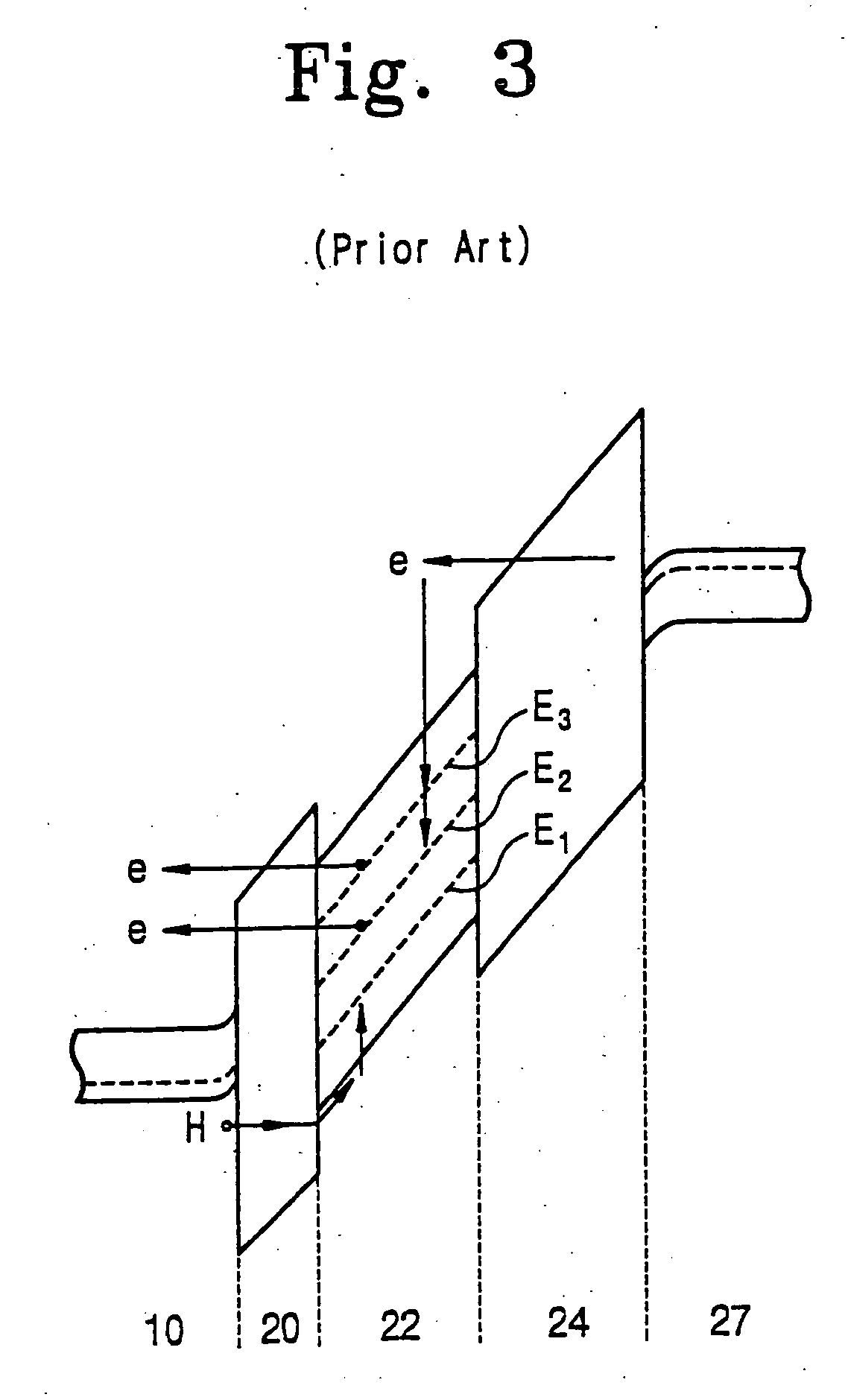
[0046] An energy band diagram of a floating trap type memory device according to some embodiments of the...
PUM
Abstract
Non-volatile memory devices and methods of operating the same are disclosed. A non-volatile memory device includes a semiconductor substrate. A tunnel insulating layer and a gate electrode are on the semiconductor substrate. A multiple tunnel insulation layer with a plurality of layers, a charge storage insulation layer, and a multiple blocking insulation layer with a plurality of layers are sequentially stacked between the gate electrode and the tunnel insulating layer. A first diffusion region and a second diffusion region in the semiconductor substrate are adjacent to opposite respective sides of the gate electrode. When a voltage is applied to the gate electrode and the semiconductor substrate to form a voltage level difference therebetween, a minimum field in the tunnel insulation layer is stronger than a minimum field in the blocking insulation layer. A minimum field established at a blocking insulation layer can be stronger than a minimum field established at a tunnel insulation layer, and the migration probability of charges through the tunnel insulation layer can be higher than that of charges through the blocking insulation layer. Therefore, it may be possible to use lower operation voltages, obtain higher program and erase speeds, and/or obtain a greater difference between threshold values of a program threshold voltage and an erase threshold voltage. As a result, a multi-valued non-volatile memory device may be formed therefrom.
Description
RELATED APPLICATIONS [0001] This application is a continuation-in-part of U.S. patent application Ser. No. 10 / 795,537, filed Mar. 8, 2004, which is a continuation-in-part of U.S. patent application Ser. No. 10 / 184,328, filed Jun. 27, 2002, and which is related to and claims priority from Korean Patent Application No. 2003-26776, filed on Apr. 28, 2003, from Korean Patent Application No. 2002-05622, filed on Jan. 31, 2002, and from Korean Patent Application No. 2001-37421, filed on Jun. 28, 2001, and this application is related to and claims priority from Korean Patent Application No. P2005-30456, filed Apr. 12, 2005, and from Korean Patent Application No. P2005-42096, filed, May 19, 2005, the contents of each of which are herein incorporated by reference in their entirety.FIELD OF THE INVENTION [0002] The present invention relates to a non-volatile memory devices. BACKGROUND OF THE INVENTION [0003] Two types of non-volatile memory devices are floating gate type memory devices and fl...
Claims
Application Information
Patent Timeline
Application Date:The date an application was filed.
Publication Date:The date a patent or application was officially published.
First Publication Date:The earliest publication date of a patent with the same application number.
Issue Date:Publication date of the patent grant document.
PCT Entry Date:The Entry date of PCT National Phase.
Estimated Expiry Date:The statutory expiry date of a patent right according to the Patent Law, and it is the longest term of protection that the patent right can achieve without the termination of the patent right due to other reasons(Term extension factor has been taken into account ).
Invalid Date:Actual expiry date is based on effective date or publication date of legal transaction data of invalid patent.