Method for forming a FinFET by a damascene process

a damascene and finfet technology, applied in the direction of brushes, cleaning equipment, electric generators, etc., can solve the problems of increasing the absolute etch amount, inability to guarantee the doping effect, etc., to prevent or substantially reduce the short between gate electrodes, prevent damage to an active region, and reduce costs

Active Publication Date: 2005-08-04
SAMSUNG ELECTRONICS CO LTD
View PDF4 Cites 178 Cited by
  • Summary
  • Abstract
  • Description
  • Claims
  • Application Information

AI Technical Summary

Benefits of technology

[0010] Exemplary embodiments of the invention provide a method of fabricating a FinFET. The method provides a reduction of costs in using an existing conventional transistor fabricating process, and prevents or substantially reduces a short between gate electrodes by forming a gate electrode by a damascene process, together with an adequate gate electrode separation. The method is advantageous for a contact and silicide formation of source and drain regions by forming a fin only on a gate formation region. The method prevents damage to an active region in a subsequent process by not removing a mask pattern for a formation of a device isolation film.

Problems solved by technology

However, there are several problems if such a fin transistor structure is actually applied to a memory device.
In a pre-doping of a gate electrode, to prevent degradation of device current characteristic caused by gate depletion, etc., when forming an SRAM (Static Random Access Memory), etc., gate heights of upper portions and both side portions of the fin are different, thus a sufficient doping effect cannot be guaranteed.
Such a process of forming the gate electrode not only increases an absolute etch amount necessary for the formation of the gate electrode, but may also bring about a short between gate electrodes caused by a marginal gate electrode separation.

Method used


Image

  • Method for forming a FinFET by a damascene process
  • Method for forming a FinFET by a damascene process
  • Method for forming a FinFET by a damascene process

Examples


Embodiment Construction

[0014] Exemplary embodiments of the invention are more fully described in detail with reference to the accompanied drawings. The invention may be embodied in many different forms and should not be construed as being limited to the exemplary embodiments set forth herein. Rather, these exemplary embodiments are provided so that this disclosure is thorough and complete, and to convey the concept of the invention to those skilled in the art.

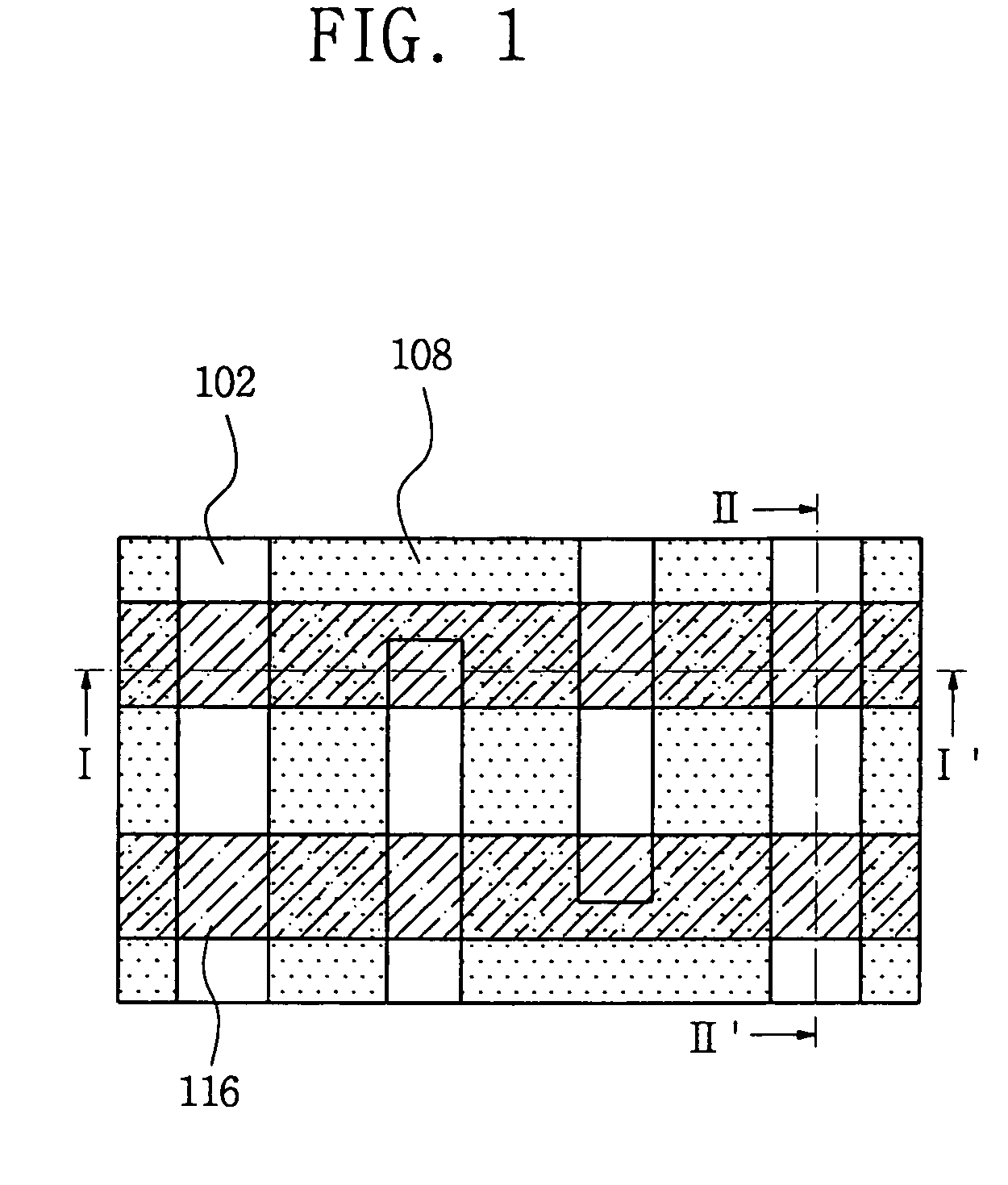
[0015]FIG. 1 is a layout of a FinFET according to an exemplary embodiment of the invention.

[0016] Referring to FIG. 1, an active region 102 formed on a semiconductor substrate is defined by a device isolation film 108, and a gate electrode is formed on a portion of the active region 102.

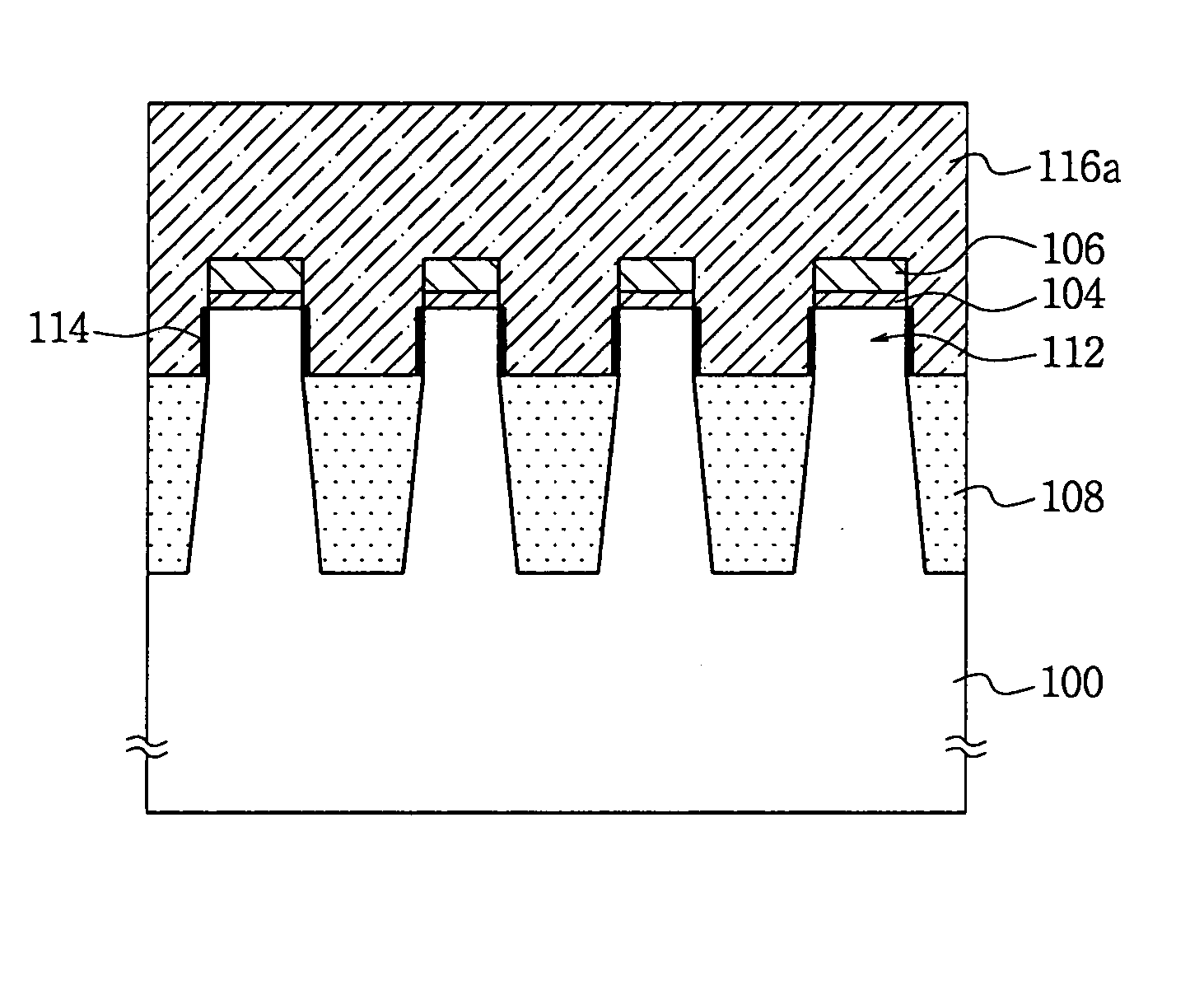
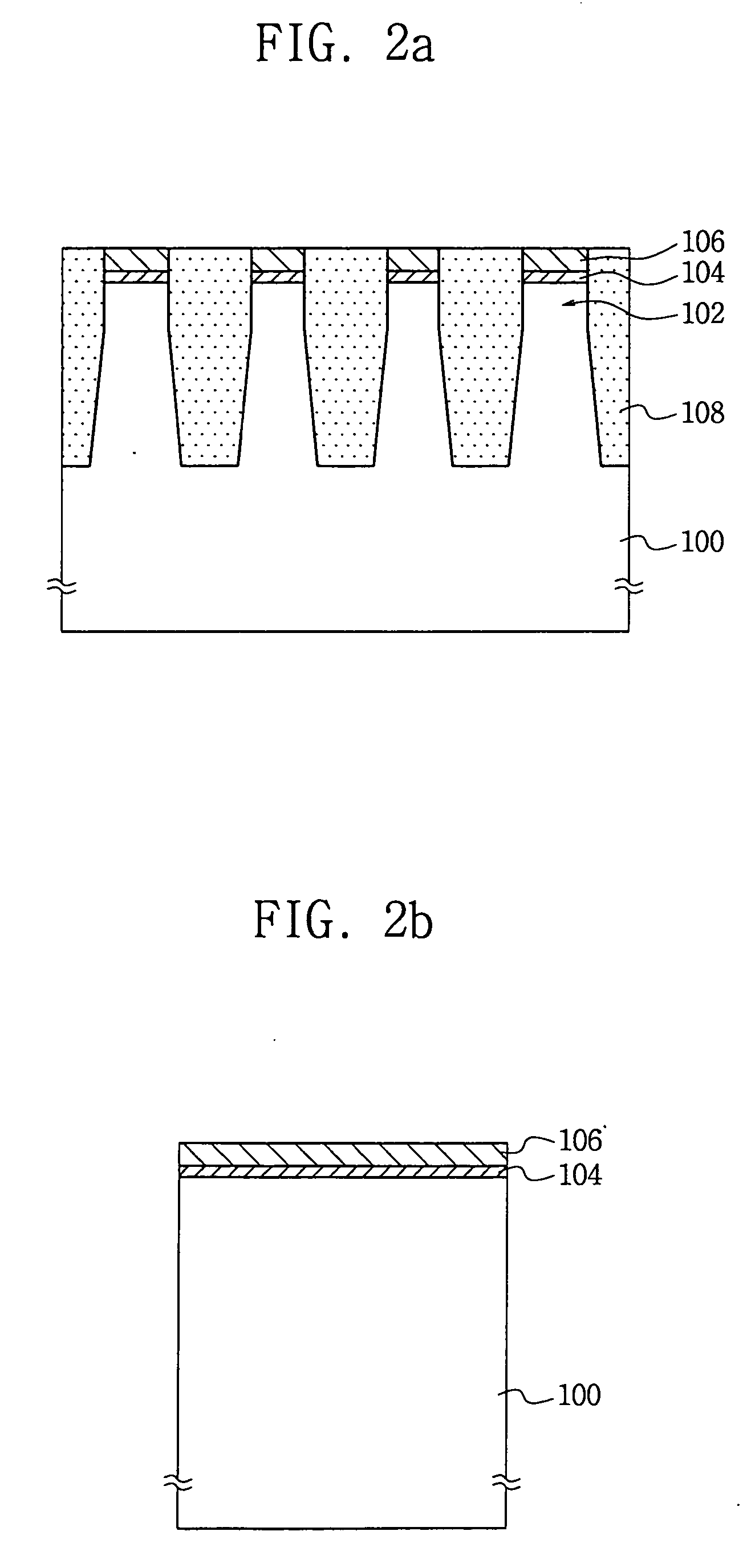
[0017] For reference, in FIGS. 2a to 8b, the drawing numbers with a character ‘a’ are cross-sectional views taken along line I-I′ in FIG. 1, and the drawing numbers with a character ‘b’ are cross-sectional views taken along line II-II′ in FIG. 1.

[0018] Referring t...


PUM

PropertyMeasurementUnit
thicknessaaaaaaaaaa
heightaaaaaaaaaa
anisotropicaaaaaaaaaa

Abstract

A device isolation film and an active region are formed on a semiconductor substrate, using a first mask pattern to expose only a formation region of the device isolation film. Only the device isolation film is selectively etched by using the first mask pattern and a second mask pattern as an etch mask, to form a fin only on a gate formation region, the second mask pattern to expose only a gate electrode formation region. A gate insulation layer is formed on both sidewalls of the fin and a gate electrode covering the first mask pattern and the gate insulation layer is formed. Source and drain regions are formed on the remaining portion of the active region where the gate electrode was not formed. Gate electrode separation becomes adequate and manufacturing costs can be reduced.

Description

CROSS REFERENCE TO RELATED APPLICATIONS [0001] This application claims priority from Korean Patent Application No. 2004-6557, filed on Feb. 2, 2004, the contents of which are hereby incorporated by reference for all purposes. BACKGROUND OF THE INVENTION [0002] 1. Field of the Invention [0003] This disclosure relates to the manufacturing of semiconductor devices, and more particularly, to a method of manufacturing an FinFET by a damascene process. [0004] 2. Description of the Related Art [0005] Metal oxide semiconductor field effect transistors (MOSFET) have been increasingly miniaturized for higher performance and integration. For an integration increase of such a device, new techniques have been constantly proposed. This has brought about a development of devices prominent in their aspects of operation and size. [0006] A technique to enhance an integration of a fin field effect transistor (FinFET) has been proposed. In this FinFET, a body region of a transistor is formed by a verti...

Claims


Application Information

Patent Timeline
Patent Type & Authority Applications(United States)
IPC IPC(8): H01L27/092H01L21/336H01L21/8228H01L29/786H01M8/00
CPCH01L29/7851H01L29/66795A46B11/0062A46B2200/306A47L23/08
Inventor KANG, HEE-SOOLEE, CHULKIM, TAE-YONGPARK, DONG-GUNAHN, YOUNG-JOONLEE, CHOONG-HOHAN, SANG-YEON
Owner SAMSUNG ELECTRONICS CO LTD
Why Eureka
Try Eureka