Semiconductor device manufacturing method

a manufacturing method and semiconductor technology, applied in the direction of semiconductor devices, basic electric elements, electrical appliances, etc., can solve the problems of decreasing the efficiency of increasing the number of operations, and achieve the effect of appropriate and efficient manufacturing a semiconductor devi

Inactive Publication Date: 2011-02-17
TOKYO ELECTRON LTD
View PDF11 Cites 176 Cited by
  • Summary
  • Abstract
  • Description
  • Claims
  • Application Information

AI Technical Summary

Benefits of technology

[0012]To solve the above and / or other problems, the present invention provides a method of appropriately and efficiently manufacturing a semiconductor device.

Problems solved by technology

When the etching process is performed in two steps as described above, the etching process needs to be performed in different conditions, and thus number of operations increases, thereby decreasing the efficiency of manufacturing a semiconductor device.

Method used


Image

  • Semiconductor device manufacturing method
  • Semiconductor device manufacturing method
  • Semiconductor device manufacturing method

Examples


Embodiment Construction

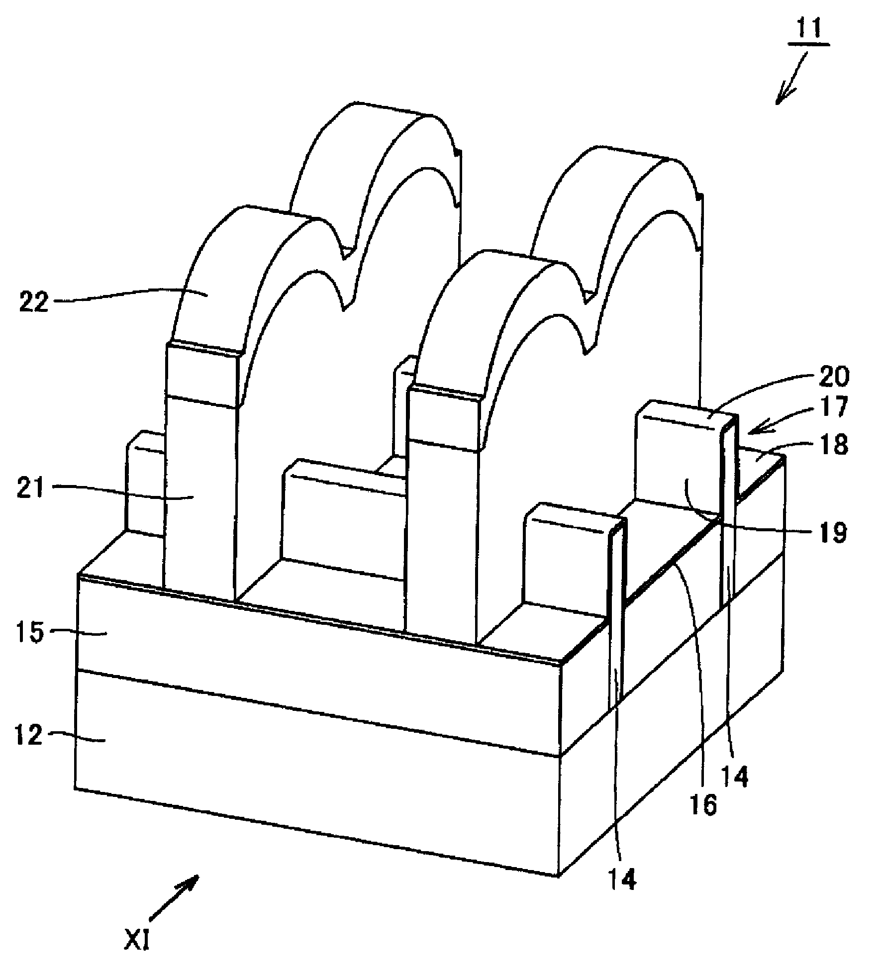
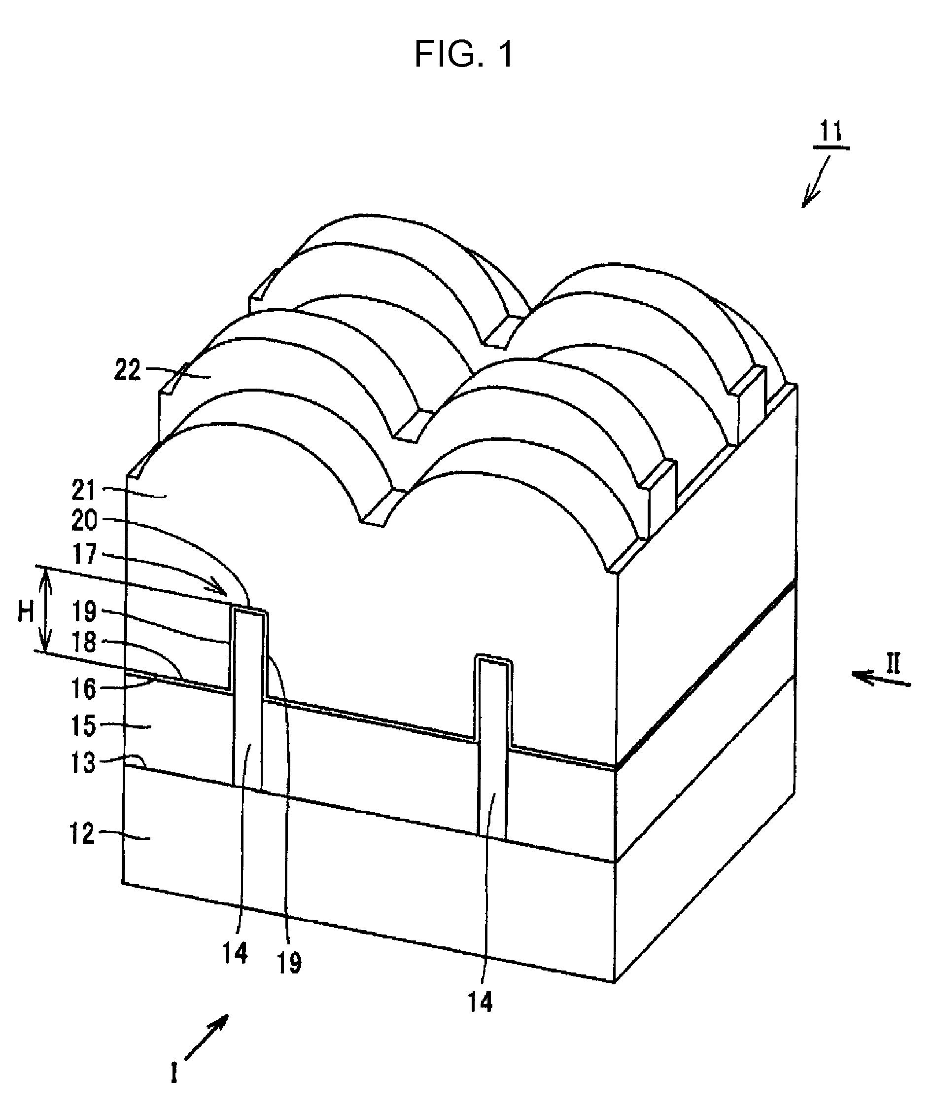
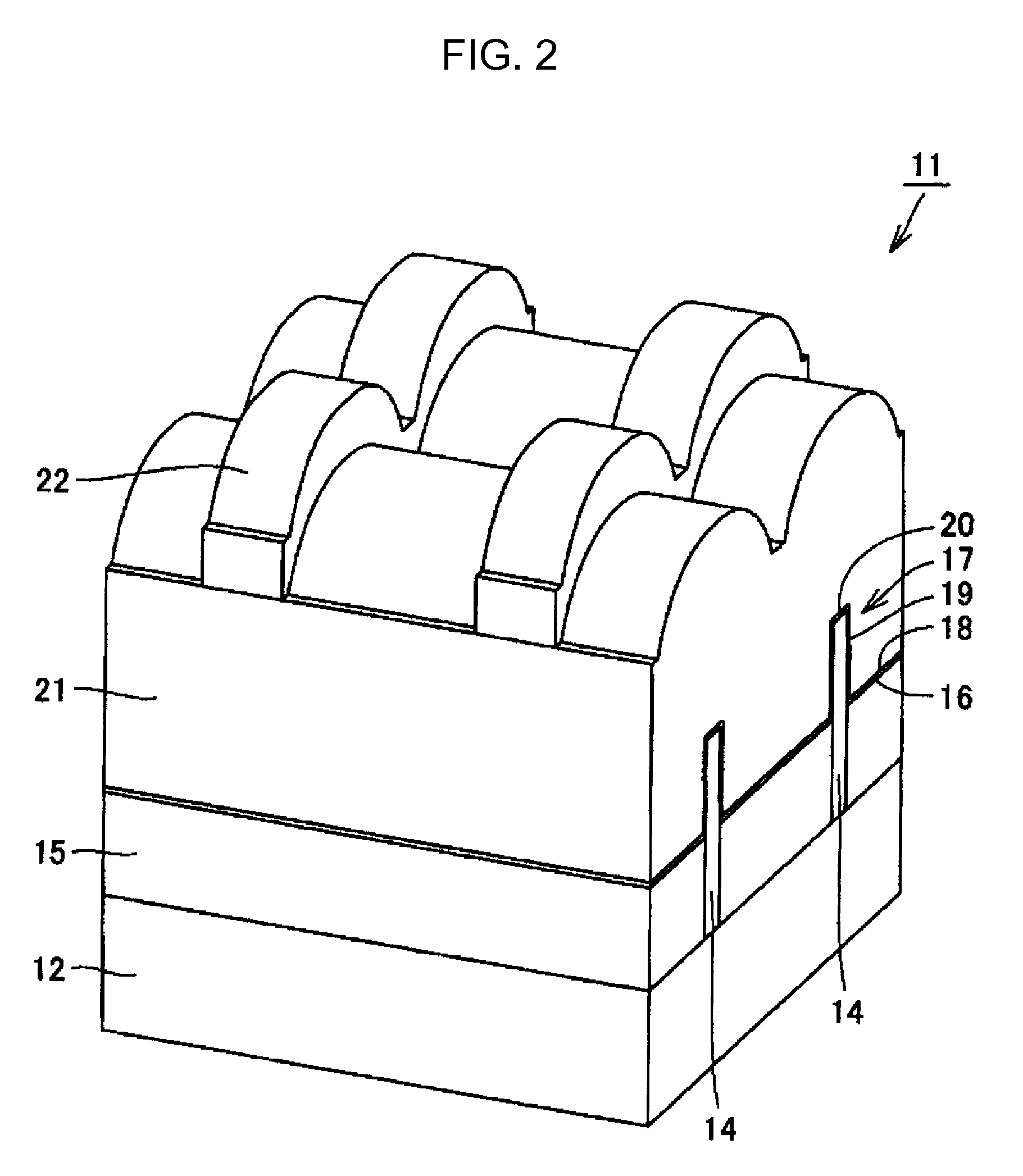
[0035]Hereinafter, the present invention will be described in detail by explaining exemplary embodiments of the invention with reference to the attached drawings.

[0036]FIGS. 1 through 4 are exterior perspective views for explaining a semiconductor device 11 manufactured according to a semiconductor device manufacturing method of an embodiment of the present invention. FIG. 1 shows a conductive layer 21 before an etching process is performed, and FIG. 2 shows the semiconductor device 11 of FIG. 1, viewed from a direction of an arrow II of FIG. 1. FIG. 3 shows the conductive layer 21 after the etching process is performed, and FIG. 4 shows the semiconductor device 11 of FIG. 3, viewed from a direction of an arrow IV of FIG. 3. The semiconductor device 11 manufactured according to the method of the present embodiment may be a semiconductor device including a metal oxide semiconductor (MOS) transistor having a is 3-dimensional structure, and an apparatus for performing the etching proce...


PUM


Abstract

A semiconductor device manufacturing method, the method including: forming an insulation layer having a protruding portion, the insulation layer having a surface and a rising surface that protrudes upward from the surface, on a semiconductor substrate; forming a conductive layer to cover the insulation layer having the protruding portion; and removing a predetermined region of the conductive layer by patterning the predetermined region according to an etching process using microwave plasma, which uses a microwave as a plasma source, while applying bias power of 70 mW/cm2 or above on the semiconductor substrate, under a high pressure condition of 85 mTorr or above.

Description

TECHNICAL FIELD[0001]The present invention relates to a semiconductor device manufacturing method, and more particularly, to a semiconductor device manufacturing method, the method including an operation of performing an etching process by using plasma.BACKGROUND ART[0002]Semiconductor devices, such as large scale integrated circuits (LSI), are manufactured by alternately stacking an insulation layer and a conductive layer on a semiconductor substrate. Generally, a layer formed on the semiconductor substrate through a chemical vapor deposition (CVD) process, or the like is patterned according to an etching process, thereby stacking layers on the semiconductor substrate. During is the etching process, plasma generated by various devices, such as a parallel plate plasma plasma source, an inductively-coupled plasma (ICP) plasma source, and an electron cyclotron resonance (ECR) plasma source is used.[0003]Recently, in semiconductor devices including a semiconductor element, such as a me...

Claims


Application Information

Patent Timeline
Patent Type & Authority Applications(United States)
IPC IPC(8): H01L21/336
CPCH01L21/32137H01L29/66795H01L21/306H01L21/28H01L29/785H01L21/28008
Inventor NISHIZUKA, TETSUYATAKAHASHI, MASAHIKO
Owner TOKYO ELECTRON LTD
Why Eureka
Try Eureka