LED array package structure having silicon substrate and method of making the same

a silicon substrate and array package technology, applied in the direction of basic electric elements, electrical equipment, semiconductor devices, etc., can solve the problems of reducing the manufacturing cost, and the precision of the assembly machine used for packaging, so as to reduce the manufacturing cost and increase the light utility

Inactive Publication Date: 2008-08-14
TOUCH MICRO SYST TECH
View PDF3 Cites 179 Cited by
  • Summary
  • Abstract
  • Description
  • Claims
  • Application Information

AI Technical Summary

Benefits of technology

[0008]It is therefore an object of the present invention to provide an LED array package structure having a silicon substrate and a method making the same so as to increase light utility and reduce the manufacturing cost.

Problems solved by technology

Also, the assembly machine used for packaging has a limitation in precision of die attachment, so the distance 40 between the LEDs 30 is more than 100 μm.
Further, the LED array package structure 10 cannot be applied to a product needing a light source with high resolution, such as liquid crystal display etc.
But, the machining method has a limitation so that the method of using the cup-structure cannot improve the assembly size in spite of having a function of condensing light.
However, the illumination area of the large-sized LED is too large so that a part of the light will be totally reflected in the LED so as to reduce the illumination efficiency.
Additionally, although a thin GaN technology used to make extremely thin sidewalls of an LED is a method utilized to reduce the light emitted from the side surfaces of the LED and to increase the light emitted from the top surface of the LED, the cost of the thin GaN technology is much more expensive than the ordinary technology.

Method used


Image

  • LED array package structure having silicon substrate and method of making the same
  • LED array package structure having silicon substrate and method of making the same
  • LED array package structure having silicon substrate and method of making the same

Examples


Embodiment Construction

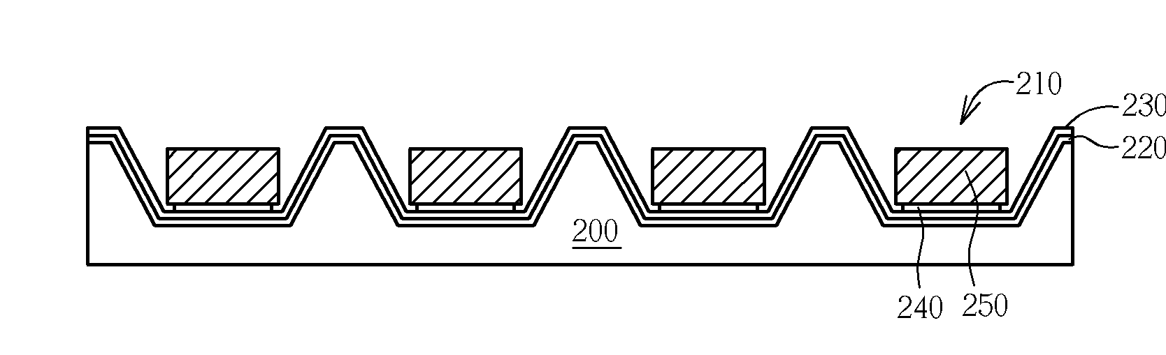
[0018]FIG. 3 is a cross-sectional schematic diagram of an LED array package structure having a silicon substrate. The LED array package structure 100 includes a silicon substrate 110 having a plurality cup-structures 120 thereon, a reflective layer 130 disposed on the silicon substrate 110 and covering the surface of each cup-structure 120, a transparent insulating layer 140 disposed on the reflective layer 130, a conductive layer 150 disposed on the transparent insulating layer 140 and a plurality of LEDs 160 respectively disposed on the transparent insulating layer 150 in each cup-structure 120, wherein each cup-structure 120 has inclined sidewalls, and the function of the sidewalls is used to reflect the scattering sidelight emitted from the side surfaces of the LEDs 160 and change the direction of the scattering sidelight to the upward direction. If a specific optical effect of the LED array package structure 100 is required, the effect can be achieved by adjusting depth, width,...


PUM


Abstract

An LED array package structure having a silicon substrate is disclosed. The LED array package structure comprises a silicon substrate having a plurality of cup-structures thereon, a reflective layer disposed on the silicon substrate, a transparent insulation layer disposed on the reflective layer, a conductive layer disposed on the transparent insulation layer and a plurality of LEDs disposed respectively on the conductive layer in each cup-structures.

Description

BACKGROUND OF THE INVENTION [0001]1. Field of the Invention[0002]The present invention relates to a light emitting diode (LED) array package and a method of making the same, and more particularly, to an LED array package having a silicon substrate with cup-structures and a method of making the same by utilizing a microelectromechanical process or semiconductor process.[0003]2. Description of the Prior Art[0004]Since the LED has advantages of a long lifetime, a small size, a high resistance to shock, a low heat emission, and a low consumption of electrical power, the LED is widely applied as a pilot lamp or a light source for various household appliances and instruments. Additionally, the LED has been developed toward producing colorful lights and high brightness in recent years, so that the LED is further applied in many kinds of movable or large-sized electronic products ranging from being a back light source of a display, lamp, traffic signals and outside colorful signboards to be...

Claims


Application Information

Patent Timeline
Patent Type & Authority Applications(United States)
IPC IPC(8): H01L21/00H01L33/00H01L33/46
CPCH01L25/0753H01L33/46H01L2924/0002H01L2924/00
Inventor LIN, HUNG-YICHANG, HONG-DA
Owner TOUCH MICRO SYST TECH
Why Eureka
Try Eureka