Lead frame of high-power chip package structure and manufacturing method thereof

A technology of chip packaging and manufacturing methods, applied in semiconductor/solid-state device manufacturing, semiconductor devices, semiconductor/solid-state device components, etc., can solve problems such as high risk of burnout, large amount of materials, and fast local deterioration of the adhesive layer

Active Publication Date: 2011-08-10
ADVANCED SEMICONDUCT ENG (WEIHAI) INC
View PDF9 Cites 8 Cited by
  • Summary
  • Abstract
  • Description
  • Claims
  • Application Information

AI Technical Summary

Problems solved by technology

In this way, the adhesive layer 14 is prone to local deterioration due to uneven heating, and may cause delamination locally
Once peeling occurs, the high heat generated by the chip 13 will not be able to dissipate heat downward in time, and there is a very high risk of burning, thus relatively reducing the reliability and service life of the packaging structure 10
In addition, if there is no anti-tilt structure in the groove 111, when the adhesive material of the adhesive layer 14 is designed to reach a certain thickness, not only the amount of material used is relatively large, but also relatively soft, and it is very easy to be squeezed out. Glue overflow occurs, thereby polluting the bonding quality of the grounding area on the upper surface of the chip holder 11

Method used


Image

  • Lead frame of high-power chip package structure and manufacturing method thereof
  • Lead frame of high-power chip package structure and manufacturing method thereof
  • Lead frame of high-power chip package structure and manufacturing method thereof

Examples


Embodiment Construction

[0036] The following descriptions of the various embodiments refer to the accompanying drawings to illustrate specific embodiments in which the present invention can be practiced. Furthermore, the directional terms mentioned in the present invention, such as "up", "down", "front", "back", "left", "right", "inside", "outside" or "side", etc., It is only for orientation with reference to the attached drawings. Therefore, the directional terms used are used to illustrate and understand the present invention, but not to limit the present invention.

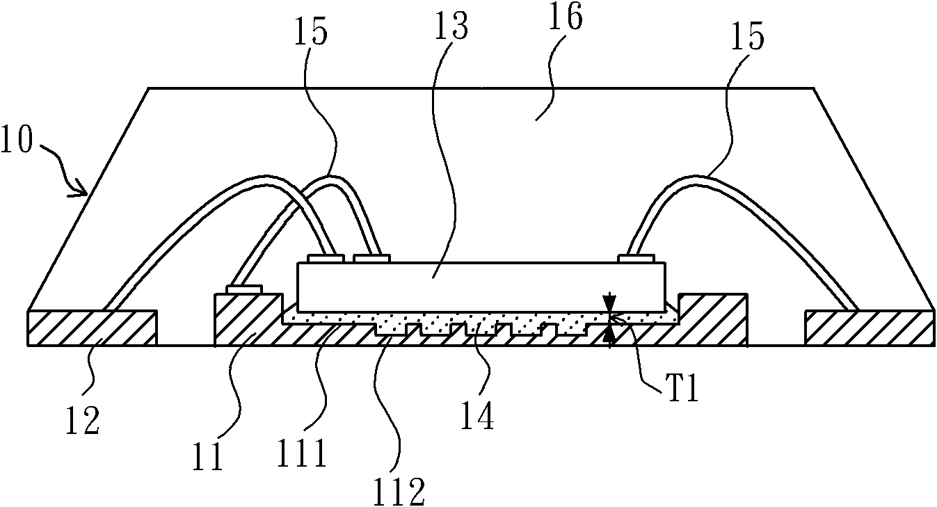
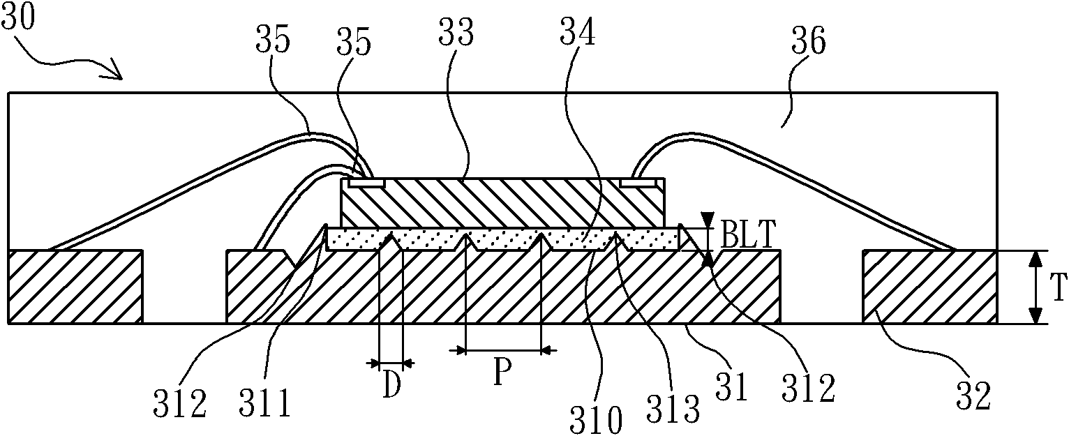
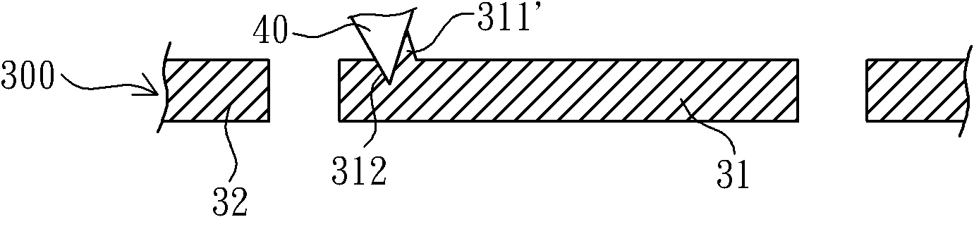
[0037] Please refer to figure 2 As shown, it discloses the high-power chip packaging structure 30 of the first embodiment of the present invention, which mainly includes a chip holder 31, several contacts 32, a high-power chip 33, an adhesive layer 34, several wires 35 and a Packaging adhesive 36, wherein the chip holder 31 and several contacts 32 are collectively referred to as a lead frame (unit), the present invention will be us...


PUM


Abstract

The invention discloses a lead frame of a high-power chip package structure and a manufacturing method thereof. A chip holder of the lead frame has a thickness of at least 0.5mm, so that sufficient heat absorbing efficiency and heat dissipation efficiency can be provided. The chip holder is also provided with an accommodating space for accommodating an adhesive layer, and a plurality of bumps are arranged at the inner bottom of the accommodating space, so that the lower surface of a high-power chip is prevented from tilting and an adhesive material in the accommodating space is prevented from overflowing, the levelness of the high-power chip is maintained, and the adhesion thickness of the adhesive layer is effectively and uniformly controlled. Therefore, the uniformity of heat energy conduction of the adhesive layer is favorably kept, furthermore, the reliability of the high-power chip package structure is relatively improved, and the service life is relatively prolonged.

Description

technical field [0001] The present invention relates to a lead frame of a high-power chip packaging structure and a manufacturing method thereof, in particular to a lead frame of a high-power chip packaging structure capable of uniformly controlling adhesive thickness and a manufacturing method thereof. Background technique [0002] Nowadays, in order to meet the needs of various high-density packaging, the semiconductor packaging industry has gradually developed various types of packaging structures, and these packaging structures usually use leadframes or packaging substrates as the chip-carrying structures. The carrier board (carrier), where the common packaging structure using a lead frame is, for example, a small outline package structure (small outline package, SOP), a quad flat package structure (quad flat package, QFP) or a quad flat no-lead package structure ( quad flat no-leadpackage, QFN) and so on. Furthermore, when the semiconductor chip to be packaged is a hig...

Claims


Application Information

Patent Timeline
Patent Type & Authority Applications(China)
IPC IPC(8): H01L23/495H01L23/367H01L23/31H01L21/48
CPCH01L2224/32257H01L2224/32245H01L2224/73265H01L2224/48247H01L2224/83385H01L24/83H01L24/32H01L24/73H01L2224/48091H01L2224/48257H01L2924/181H01L2924/00012H01L2924/00014
Inventor 张敬模韩永一金仁浩
Owner ADVANCED SEMICONDUCT ENG (WEIHAI) INC
Why Eureka
Try Eureka