Method for testing a partially assembled multi-die device, integrated circuit die and multi-die device

An integrated circuit and multi-die technology, applied in the direction of measuring electricity, measuring devices, measuring electrical variables, etc., can solve problems such as limited test flexibility

Inactive Publication Date: 2011-08-24
NXP BV
View PDF2 Cites 12 Cited by
  • Summary
  • Abstract
  • Description
  • Claims
  • Application Information

AI Technical Summary

Problems solved by technology

Although this setup significantly improves the yield of the SiP manufacturing process, it suffers from the following

Method used


Image

  • Method for testing a partially assembled multi-die device, integrated circuit die and multi-die device
  • Method for testing a partially assembled multi-die device, integrated circuit die and multi-die device
  • Method for testing a partially assembled multi-die device, integrated circuit die and multi-die device

Examples


Embodiment Construction

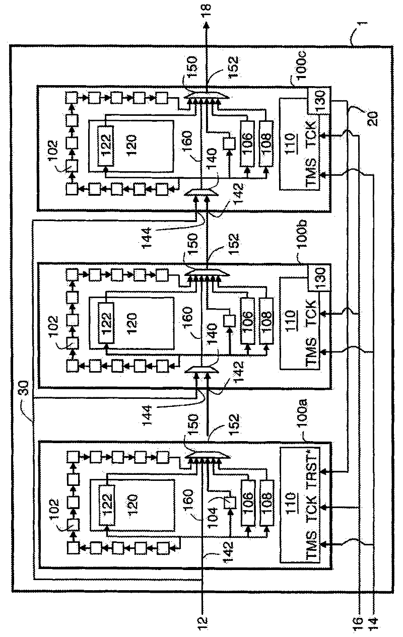
[0041] figure 1 An embodiment of a multi-die device disclosed in WO2007 / 010493 is shown that can be used to test isolated dies as well as modules as a single device in a JTAG compliant manner once the assembly of the SiP has been completed. As a non-limiting example only, device 1 is shown with 3 dies 100a-c on a carrier (not shown). The global structure of the finished multi-chip device of the present invention can be compared with figure 1 The devices shown are substantially similar, with differences discussed in more detail below.

[0042] Device 1 has multiple system interconnects, including device level TDI 12 , device level test mode select (TMS) input 14 , device level test clock (TCK) input 16 and device level TDO 18 . figure 1 Each of the illustrated IC dies 100 a - c is represented by a test apparatus comprising test access ports (TAPs) each having a TAP controller 110 . The TAPs of die 100a-c may each include a plurality of shift registers, such as a boundary sca...


PUM


Abstract

The present invention discloses a method of testing a partially assembled multi-die device (1) by providing a carrier (300) comprising a device-level test data input (12) and a device-level test data output (18); placing a first die on the carrier, the first die having a test access port (100c) comprising a primary test data input (142), a secondary test data input (144) and a test data output (152), the test access port being controlled by a test access port controller (110); communicatively coupling the secondary test data input (144) of the first die to the device-level test data input (12), and the test data output (152) of the first die to the device-level test data output (18); providing the first die with configuration information to bring the first die in a state in which the first die accepts test instructions from its secondary test data input (144); testing the first die, said testing including providing the secondary test data input (144) of the first die with test instructions through the device-level test data input (12); and collecting a test result for the first die on the device-level test data output (18). Consequently, a die of a partially assembled multi-die device such as a System-in-Package may be tested using its integrated boundary scan test architecture.

Description

technical field [0001] The present invention relates to a method for testing a partially assembled multi-die device, such as a partially assembled system-in-package (SiP). [0002] The invention also relates to an integrated circuit (IC) die for use in such a method. [0003] The invention also relates to a multi-die device comprising at least one such IC die. Background technique [0004] Due to the ever-evolving semiconductor market and technology, new semiconductor products appear in the market on a regular basis. An example of such a product gaining commercial attention is the so-called system-in-package (SiP), in which multiple discrete semiconductor dies, such as integrated circuits (ICs), are mounted on a (passive) substrate and packed into a single In package. Thus, a device is obtained that has the look and feel of a single device, unlike eg a printed circuit board (PCB) where the individual different dies on the PCB are easily identified and accessed. [0005] ...

Claims


Application Information

Patent Timeline
IPC IPC(8): G01R31/3185
CPCG01R31/318555G01R31/318558G01R19/00G01R31/26G01R31/28G01R31/31717G01R31/3183G01R31/3185G01R31/31924
Inventor 弗兰西斯库斯·杰拉德斯·玛丽亚·德·琼亚历山大·塞巴斯蒂安·比文格
Owner NXP BV
Why Eureka
Try Eureka