
Time sequence control circuit and front-end bus power supply with time sequence control circuit
一种时序控制电路、电源的技术,应用在数据处理电源、电数字数据处理、测量装置等方向,能够解决电脑无法开机、自动重启、不适用等问题,达到防止无法开机或者自动重启的效果
- Summary
- Abstract
- Description
- Claims
- Application Information
AI Technical Summary
Problems solved by technology
Method used
Image

Examples
Embodiment Construction
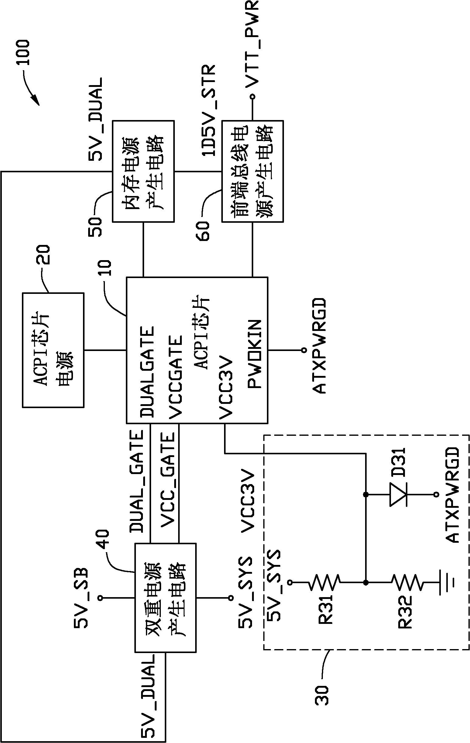
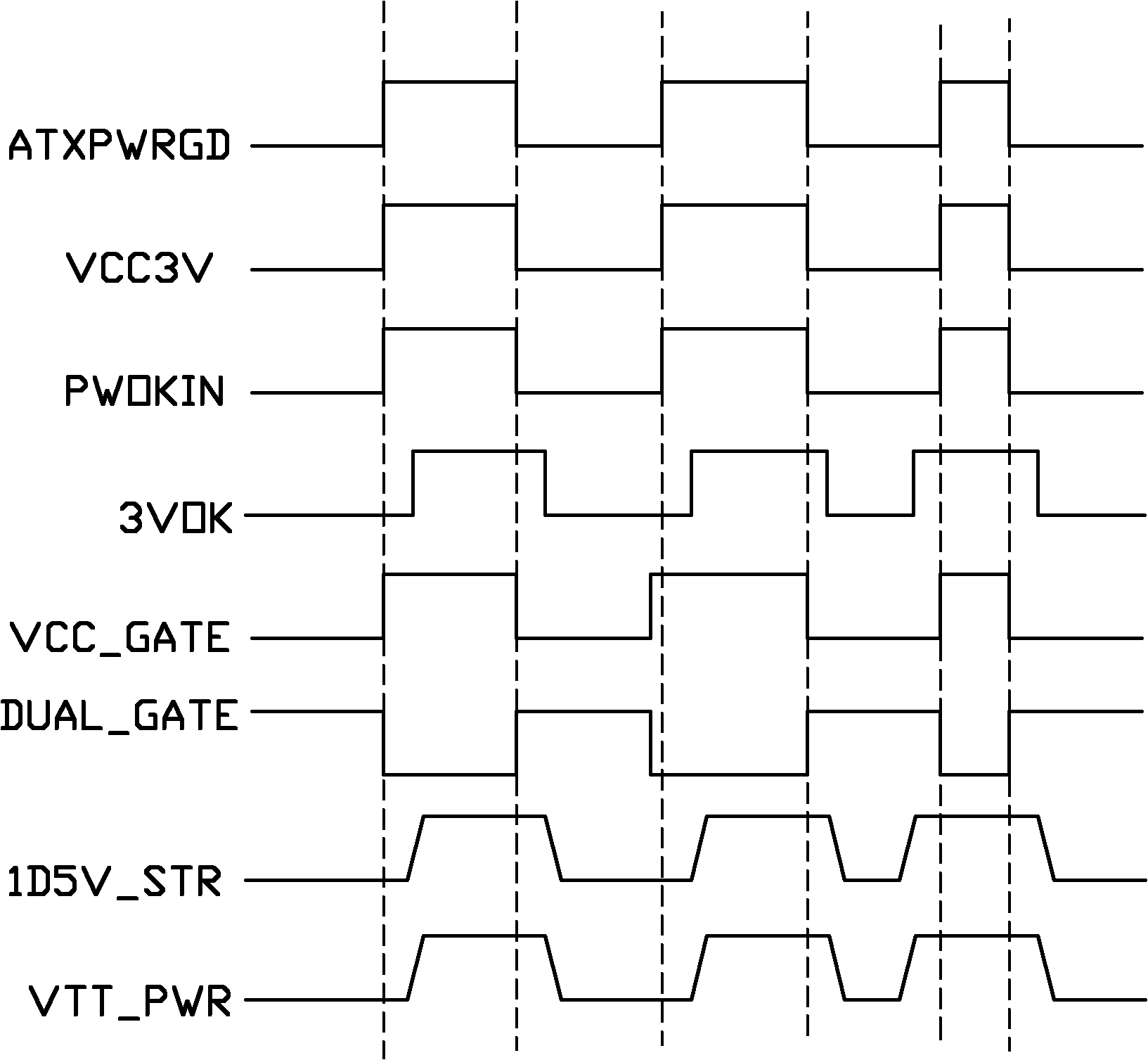
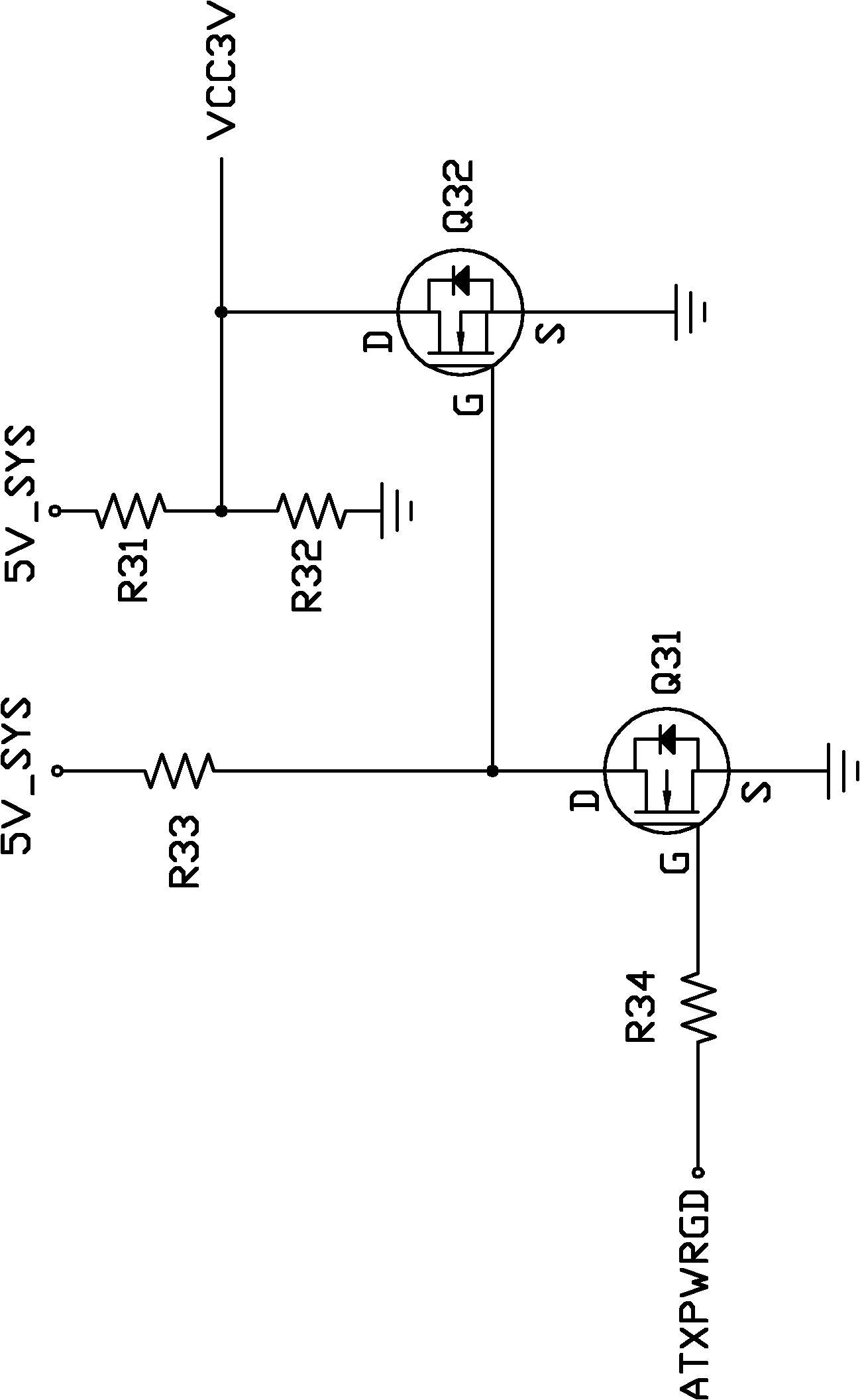
[0032] see figure 1 The FSB power supply 100 of the preferred embodiment of the present invention includes an ACPI chip 10, an ACPI chip power supply 20, a timing control circuit 30, a dual power supply generating circuit 40, a memory power generating circuit 50 and a FSB power generating circuit 60. The ACPI chip power supply 20 , timing control circuit 30 , dual power supply generation circuit 40 , memory power generation circuit 50 and FSB power generation circuit 60 are all electrically connected to the ACPI chip 10 . The ACPI chip power supply 20 can convert the voltage provided by the system power supply (not shown) into the working voltage required by the ACPI chip 10 . The timing control circuit 30 provides a timing control signal VCC3V for the ACPI chip 10 . The dual power generation circuit 40 is electrically connected to the memory power generation circuit 50 , and provides an input voltage signal 5V_DUAL for the memory power generation circuit 50 as an input powe...
PUM
 Abstract
Description
Claims
Application Information