Method for manufacturing master board and TFT (Thin Film Transistor) array substrate

A manufacturing method and array substrate technology, applied in semiconductor/solid-state device manufacturing, optics, instruments, etc., can solve the problems of product qualification rate and yield reduction, TFT array substrate electrostatic breakdown, potential difference, etc., to improve the qualification rate and Yield rate, the effect of reducing electrostatic breakdown phenomenon

Inactive Publication Date: 2014-08-20
BOE TECH GRP CO LTD +1
View PDF3 Cites 2 Cited by
  • Summary
  • Abstract
  • Description
  • Claims
  • Application Information

AI Technical Summary

Problems solved by technology

[0003] In the process of realizing the existing TFT array substrate manufacturing process, the inventor found that there are at least the following problems in the prior art (CN1195117A is the closest prior art): the TFT array substrate will accumulate more on the metal layer during the manufacturing process. The gate metal layer and the source / drain metal layer on the TFT array substrate manufactured by the existing process are completely separated by the gate insulating layer, and a potential difference is easily formed between the two metal layers due to the accumulation of charges , so that the TFT array substrate is prone to electrostatic breakdown during the manufacturing process, resulting in lower product yield and yield

Method used


Image

  • Method for manufacturing master board and TFT (Thin Film Transistor) array substrate
  • Method for manufacturing master board and TFT (Thin Film Transistor) array substrate
  • Method for manufacturing master board and TFT (Thin Film Transistor) array substrate

Examples


Embodiment 1

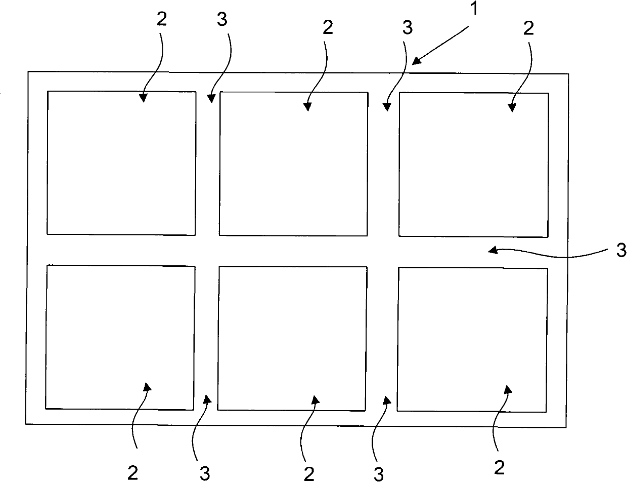
[0047] An embodiment of the present invention provides a motherboard, such as figure 1As shown, the motherboard in this embodiment includes a substrate 1 having at least one display area 2, and the periphery of the display area 2 is provided with a pre-cut area 3. After the TFT array process is completed, it is necessary to cut The region 3 is cut, and each display region 2 is cut, and each display region 2 finally forms a complete TFT array substrate. In order to reduce the electrostatic breakdown phenomenon that occurs during the manufacturing process of the TFT array substrate, the pre-cut areas on the adjacent sides of each display area of ​​the motherboard in the embodiment of the present invention are respectively provided with electrically connected gate and data communication lines, and The gate connecting lines are electrically connected to the gate scanning lines in the corresponding display area, and the data connecting lines are electrically connected to the data s...

Embodiment 2

[0078] An embodiment of the present invention provides a motherboard, the overall structure of the motherboard is the same as figure 1 Similarly, it includes a substrate with at least one display area, and a pre-cut area is provided between two adjacent display areas on the substrate. After the TFT array process is completed, it needs to be cut in the pre-cut area, and each Each display area is cut, and each display area finally forms a complete TFT array substrate.

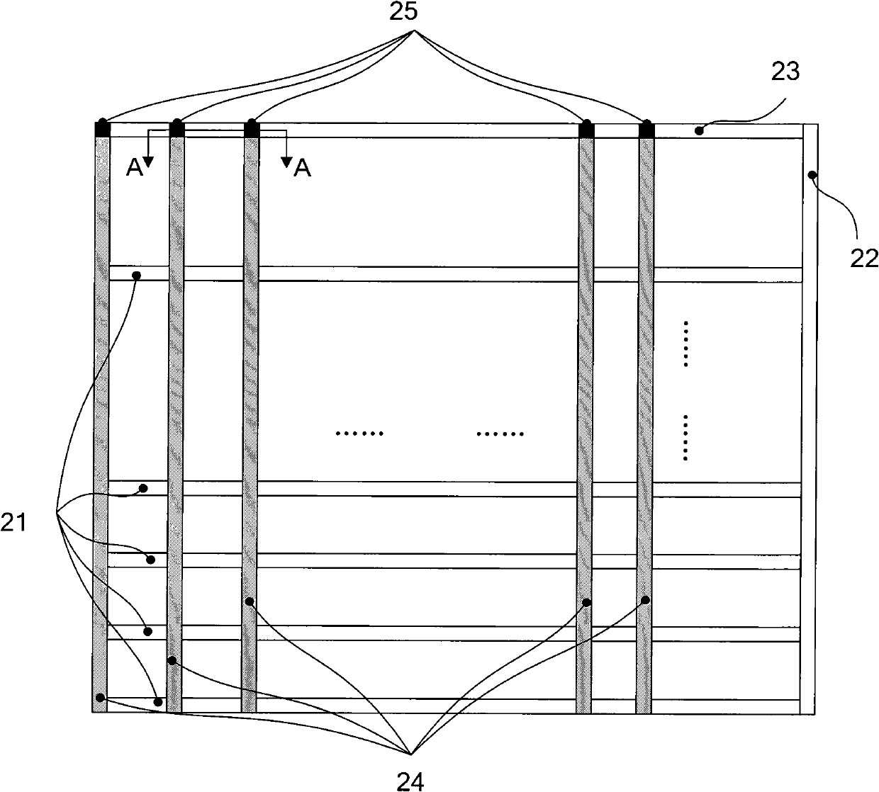
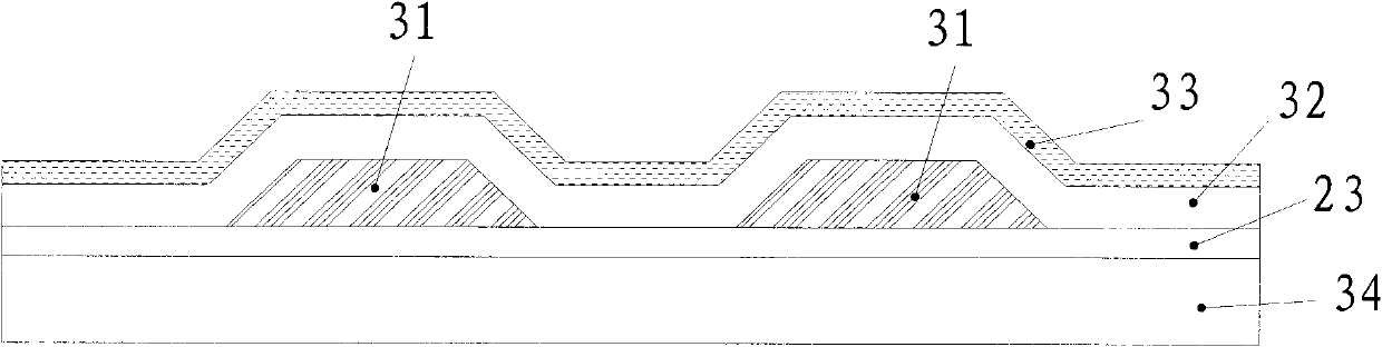
[0079] In the embodiment of the present invention, in order to reduce the electrostatic breakdown phenomenon that occurs during the manufacturing process of the TFT array substrate, a solution similar to that of embodiment 1 is adopted to electrically connect the two metal layers so that their potentials are generally equal. The following takes one of the display areas as an example to describe its specific electrical connection method in detail. Figure 6 is a schematic diagram of one of the display areas, Fi...

Embodiment 3

[0108] An embodiment of the present invention provides a motherboard, the overall structure of the motherboard is the same as figure 1 Similarly, it includes a substrate with at least one display area, and a pre-cut area is provided between two adjacent display areas on the substrate. After the TFT array process is completed, it needs to be cut in the pre-cut area, and each Each display area is cut, and each display area finally forms a complete TFT array substrate.

[0109] In the embodiment of the present invention, in order to reduce the electrostatic breakdown phenomenon that occurs during the manufacturing process of the TFT array substrate, a solution similar to that of embodiment 1 is adopted to electrically connect the two metal layers so that their potentials are generally equal. The following takes one of the display areas as an example to describe its specific electrical connection method in detail. Figure 10 is a schematic diagram of one of the display areas, F...


PUM


Abstract

The present invention relates to a mother substrate and a method for manufacturing the same, the mother substrate comprising: a substrate, comprising at least one display region and pre-cutting regions in a periphery of the display region, wherein the display region comprises gate scanning lines and data scanning lines, the pre-cutting regions comprise a gate-line connecting line and a data-line connecting line electrically connected to each other, and the gate-line connecting line is electrically connected to all of the gate scanning lines in the display region, and the data-line connecting line is electrically connected to all of the data scanning lines in the display region substrate.

Description

technical field [0001] The invention relates to the technical field of liquid crystal display, in particular to a method for manufacturing a motherboard and a TFT (Thin Film Transistor, Thin Film Field Effect Transistor) array substrate. Background technique [0002] In the current manufacturing process of the TFT array substrate, the gate metal layer is first deposited and the gate pattern is etched, and then the gate insulating layer is deposited on the surface of the substrate with the gate pattern layer, and then the active layer and the source / drain metal layer are sequentially manufactured. The TFT array substrate in the array process mainly includes deposition, etching and other processes. Since the deposition equipment and etching equipment generally require a higher operating voltage, this higher operating voltage may cause the TFT array substrate to be damaged during the manufacturing process. Among them, the metal layer accumulates more charges; and the manufactur...

Claims


Application Information

Patent Timeline
Patent Type & Authority Patents(China)
IPC IPC(8): G02F1/1362G02F1/1333H01L27/02H01L21/77
CPCG02F1/136204H01L27/1218H01L27/124G02F1/133G02F1/1368G02F1/13
Inventor 刘华锋肖红玺苏顺康吴平丁汉亭
Owner BOE TECH GRP CO LTD
Why Eureka
Try Eureka