Array resistor and PCB board applied with the array resistor

A PCB board and resistor technology, applied in the direction of printed circuits and electrical components connected by resistors, non-printed electrical components, etc., can solve the problems of reducing signal quality and difficulty in wiring adjustment, so as to avoid wiring adjustment and ensure quality. , the effect of controllable spacing

Inactive Publication Date: 2012-01-18
深圳市卓怡恒通电脑科技有限公司
View PDF1 Cites 1 Cited by
  • Summary
  • Abstract
  • Description
  • Claims
  • Application Information

AI Technical Summary

Problems solved by technology

However, wiring adjustment is very difficult for high-density PCBs, and changing positions through PCB drilling and wiring will generate parasitic inductance and parasitic capacitance, which will reduce signal quality

Method used


Image

  • Array resistor and PCB board applied with the array resistor
  • Array resistor and PCB board applied with the array resistor
  • Array resistor and PCB board applied with the array resistor

Examples


Embodiment Construction

[0015] In order to further illustrate the technical means adopted by the present invention and its effects, the following describes in detail in conjunction with preferred embodiments of the present invention and accompanying drawings.

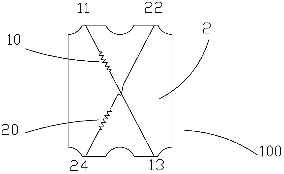
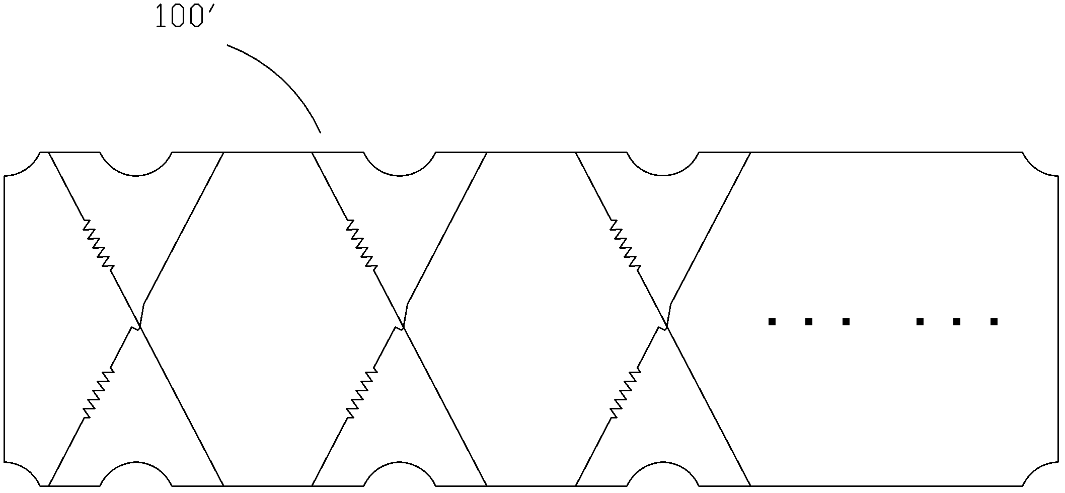
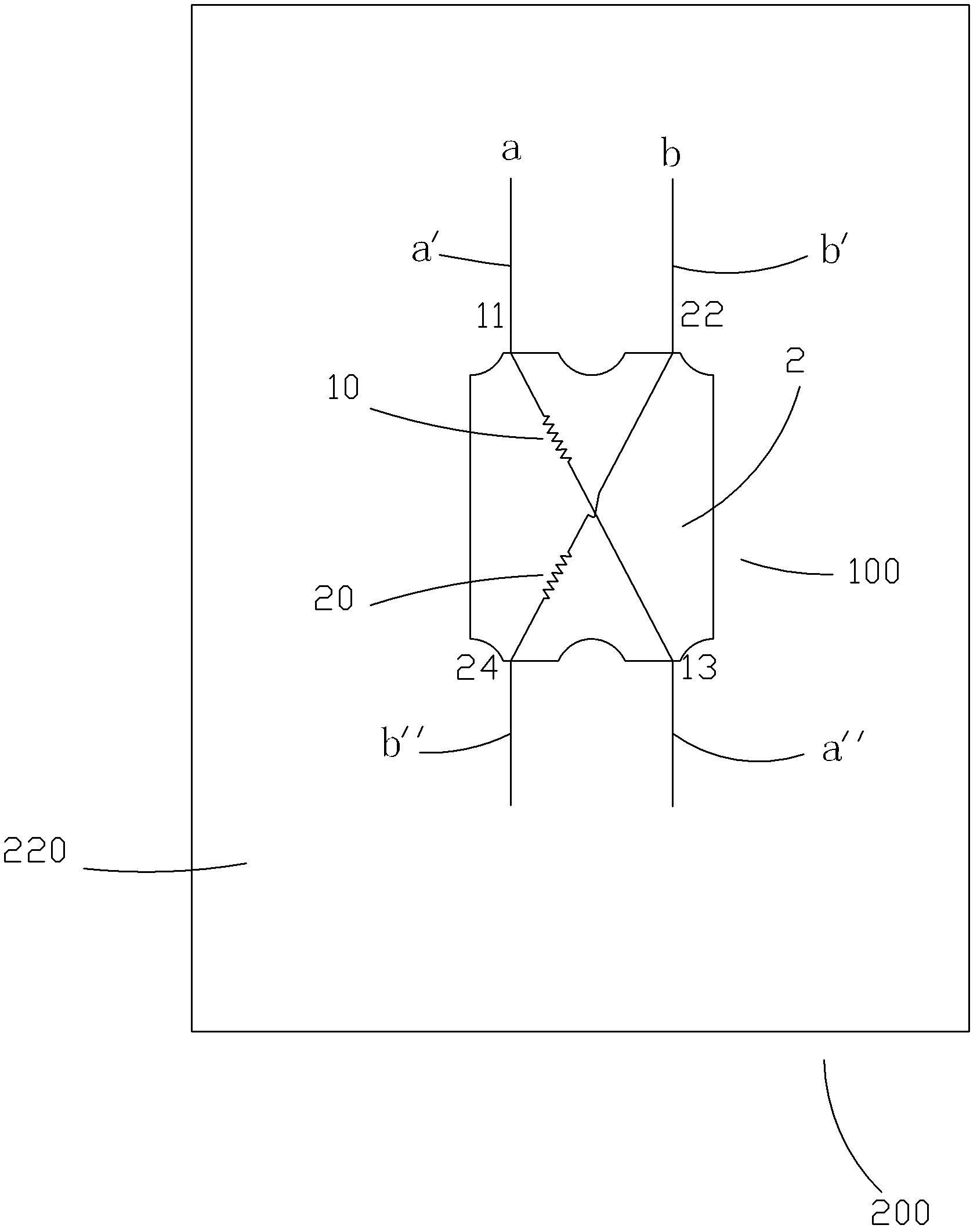
[0016] Such as figure 1 As shown, the present invention provides a resistance exclusion 100, which includes: a package body 2, and resistors 10, 20 arranged in pairs in the package body 2, the resistors 10, 20 are symmetrically crossed and insulated from each other, and the package body 2 There are pins corresponding to both ends of each resistor, and the two ends of the resistor are respectively electrically connected to the pins of the package; in this embodiment, the resistor 10 is connected to pin 11 and pin 13, and the resistor 20 is connected to pin 22 and Pin 24 is used to connect a pair of differential signal lines to form two relative paths that do not interfere with each other, so as to realize the cross-output conversion of differen...


PUM


Abstract

The invention provides an array resistor and a PCB board applied with the array resistor. The array resistor comprises a packaging body and resistors in pairs arranged in the packaging body. Resistors in each pair are symmetrically crossed and insulating with each other; two ends of each resistor are respectively provided with corresponding pins on the packaging body; and two ends of each resistor are electrically connected to packaging body pins respectively. The invention can realize crossing output transformation of signals, solve difficulty wiring and adjusting, and guarantee signal quality; meanwhile, crossing output transformation of differential signals is realize through the array resistor, so as to solve difficulty in wiring and adjusting and realize a function like a twisted pair on a board, and the array resistor is tighter than the twisted pair, has controllable spacing and amazing effect on interference inhibition.

Description

technical field [0001] The invention relates to a resistance exclusion and a PCB board using the resistance exclusion. Background technique [0002] The signal rate on the existing PCB board is getting faster and faster, the wiring density is getting higher and higher, and there are more requirements for PCB routing. The use of resistance exclusion can save space for PCB wiring, especially for high-density PCBs. Resistance exclusion is several resistors packaged together. It is more convenient to use resistance exclusion than to use several resistors, so resistance exclusion applications have been developed rapidly. The existing exclusions are all straight-through. When the differential signal crosses and the routing needs to be changed, the existing exclusions are not applicable. It is necessary to adjust the wiring or change the position through PCB punching and threading. However, wiring adjustment is very difficult for high-density PCBs, and changing positions through P...

Claims


Application Information

Patent Timeline
Patent Type & Authority Applications(China)
IPC IPC(8): H01C13/02H05K1/18
Inventor 季晓东
Owner 深圳市卓怡恒通电脑科技有限公司
Why Eureka
Try Eureka