Wave splicing power regulating device based on MOSFET (Metal-Oxide-Semiconductor Field Effect Transistor)

A technology of power regulation and effect tube, which is applied in the direction of output power conversion device, AC power input conversion to AC power output, electrical components, etc. It can solve the problems of reducing power factor, output voltage waveform distortion, and low power utilization rate. To achieve the effect of avoiding short circuit

Active Publication Date: 2013-07-24
NANJING NENGRUI AUTOMATION EQUIP
View PDF4 Cites 0 Cited by
  • Summary
  • Abstract
  • Description
  • Claims
  • Application Information

AI Technical Summary

Problems solved by technology

The advantage of this voltage regulation method is that the output energy will not fluctuate too much, and the control accuracy is high, but the problem is that the output voltage waveform is seriously distorted, a large number of high-order harmonic components are generated, the power factor is reduced, and the power utilization rate is low. not tall
However, the power adjustment device is based on thyristor to fight the output voltage. Due to the structure of the MOSFET itself, there is an anti-parallel intrinsic diode between the drain and the source, so that between the drain and the source The device will conduct when a reverse voltage is applied between them, and this conduction is uncontrollable, so it is not suitable for MOSFET

Method used


Image

  • Wave splicing power regulating device based on MOSFET (Metal-Oxide-Semiconductor Field Effect Transistor)
  • Wave splicing power regulating device based on MOSFET (Metal-Oxide-Semiconductor Field Effect Transistor)
  • Wave splicing power regulating device based on MOSFET (Metal-Oxide-Semiconductor Field Effect Transistor)

Examples


Embodiment 1

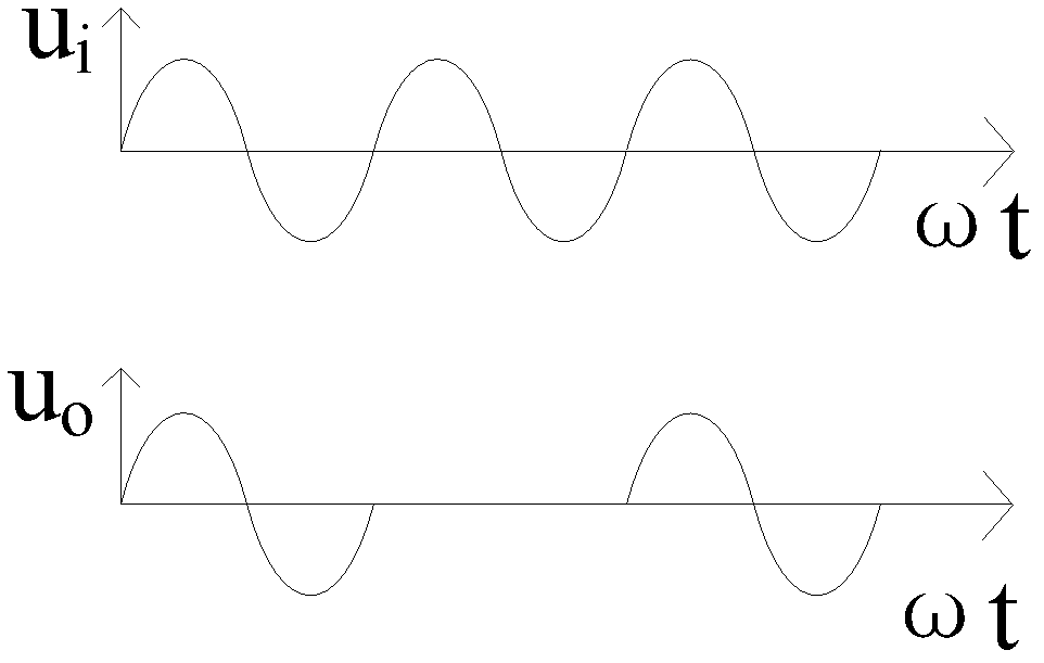
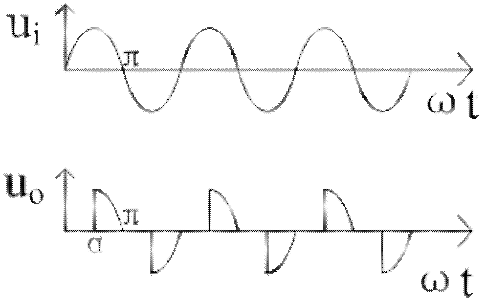
[0031] Figure 5 It is a principle diagram of a specific embodiment of the mosfet-based wave-scrambling power adjustment device of the present invention.

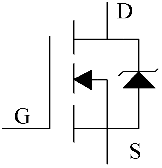
[0032] In this example, if figure 1 As shown, the mosfet-based power adjustment device of the present invention includes a transformer T, two sets of insulated gate electric field effect transistors and a controller.

[0033] Transformer T has two first-stage secondary outputs S with different transformation ratios 1 , Secondary secondary output S 2 , the primary of the transformer T is connected to the main loop of the grid V s , the two secondary outputs S 1 , S 2 Output the first stage voltage u with the same phase and different voltage 1 and the second stage voltage u 2 , where the first stage voltage u 1 Less than the second stage voltage u 2 ;

[0034] The first group and the second group of insulated gate type power field effect transistors are respectively connected to the first stage and second stage seco...


PUM


Abstract

The invention discloses a wave splicing power regulating device based on MOSFET (Metal-Oxide -Semiconductor Field Effect Transistor). The conduction angle alpha is regulated to vary in the range of 0 to pai according to required power, so that the continuous regulation of output voltage from the second level of voltage to the first level of voltage, and the regulation of power required by power utilization equipment is realized. Because each group of insulated gate field effect transistors includes a forward insulated gate field effect transistor and a reverse insulated gate field effect transistor connected in series, after each group of insulated gate field effect transistors is turned off, an output circuit formed from intrinsic diodes in series back-to-back is formed, the transistors can not be conducted to form a return circuit. Thus, the influence of intrinsic diodes in parallel back-to-back between a drain electrode and a source electrode caused by the structure of the insulated gate field effect transistors is overcome, short circuit caused by simultaneous output of two levels of secondary circuits is avoided, and MOSFET can be applied to the wave splicing power regulatingdevice.

Description

technical field [0001] The invention belongs to the technical field of power adjustment of electrical equipment, and more specifically relates to a wave-scrambling power adjustment device. Background technique [0002] Electric field effect transistors are divided into junction type and insulated gate type, usually mainly referring to insulated gate type, referred to as MOSFET. It has the characteristics of low driving power, high operating frequency, good thermal stability, small on-state impedance, and small size. It is a power semiconductor device used in power electronic circuits. [0003] MOSFET is a voltage-controlled three-terminal device, and its electrical symbol is as follows figure 1 Shown, with gate G, drain D and source S, by the gate-source voltage u GS Control the on-off between the drain and the source, and work in the switch state. When a forward voltage higher than the threshold voltage u is applied between the MOSFET gate and source GS When the drain a...

Claims


Application Information

Patent Timeline
Patent Type & Authority Patents(China)
IPC IPC(8): H02M5/293
Inventor 白利兵程玉华秦健康陈凯张杰潘虹
Owner NANJING NENGRUI AUTOMATION EQUIP
Why Eureka
Try Eureka