Liquid crystal display panel

一种液晶显示面板、阵列基板的技术,应用在静态指示器、仪器、非线性光学等方向,能够解决显示不良、产能下降等问题

Active Publication Date: 2012-02-15
AU OPTRONICS CORP
View PDF7 Cites 17 Cited by
  • Summary
  • Abstract
  • Description
  • Claims
  • Application Information

AI Technical Summary

Problems solved by technology

Since the coating of frame glue and the production of silver glue are two separate processes, the production of silver glue will reduce the throughput of thin film transistor liquid crystal display.
In addition, the silver paste often causes the cell gap of the LCD panel to be unable to be precisely controlled, resulting in poor display (mura)

Method used


Image

  • Liquid crystal display panel
  • Liquid crystal display panel
  • Liquid crystal display panel

Examples


Embodiment Construction

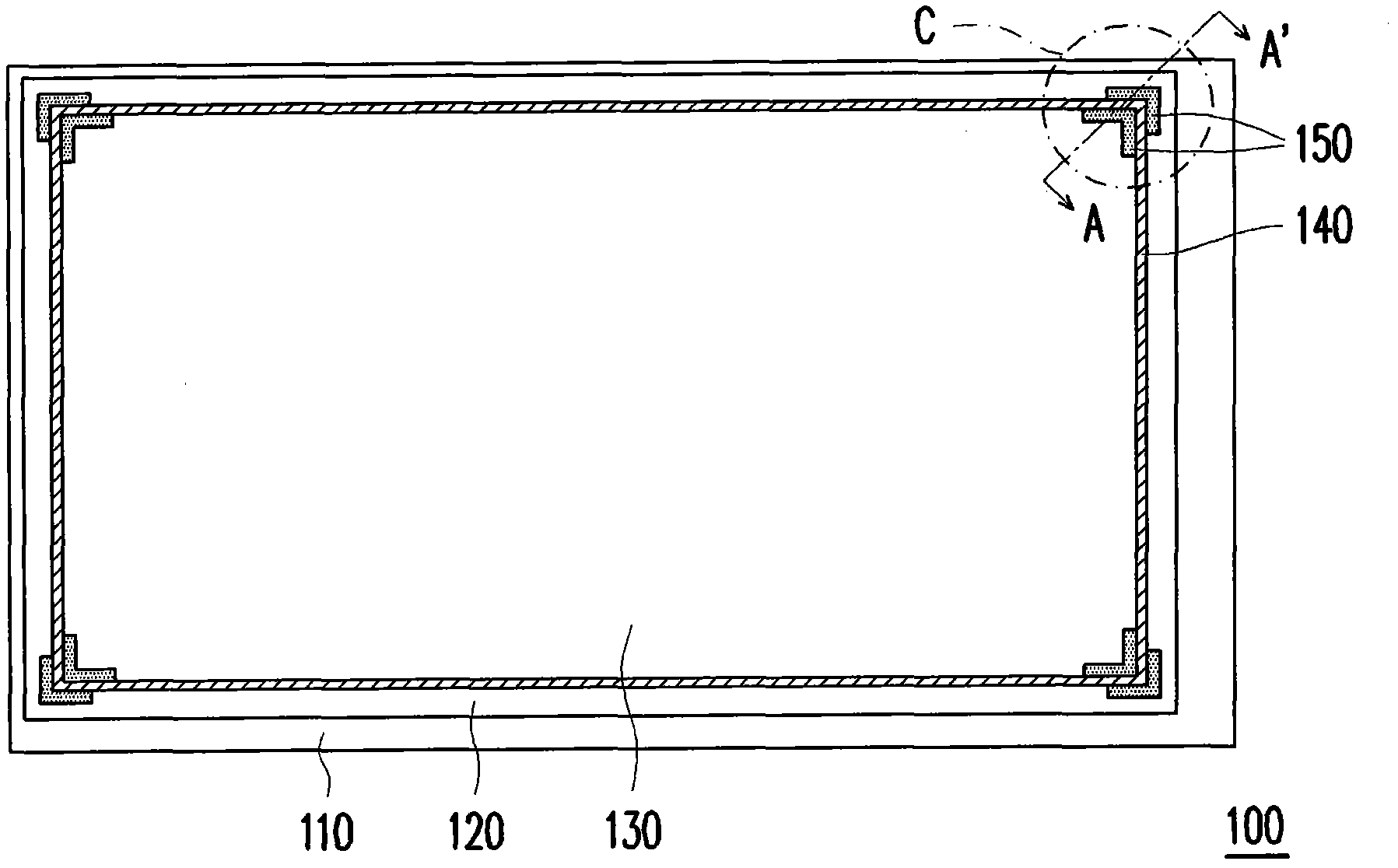
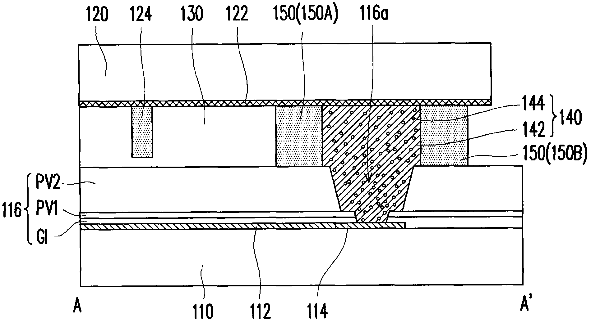
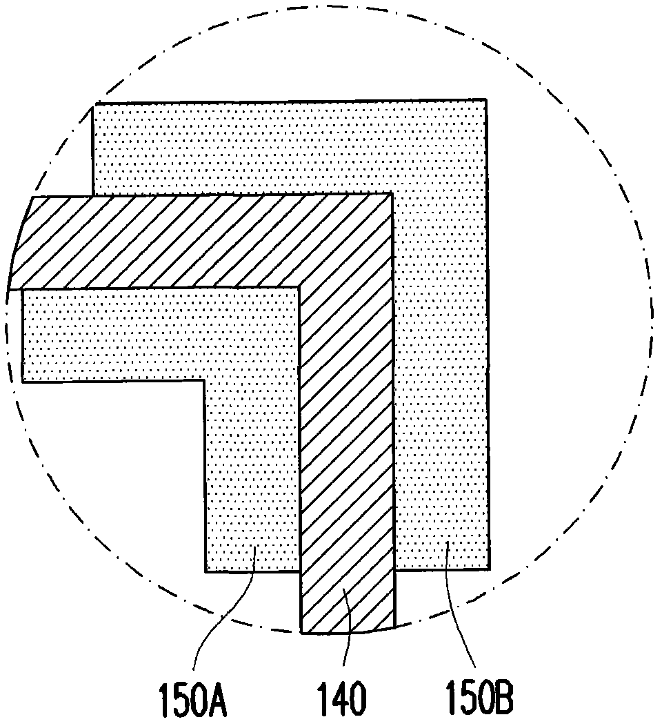
[0049] figure 1 is a schematic top view of a liquid crystal display panel according to an embodiment of the present application, and figure 2 for figure 1 Schematic sectional view along section line A-A' at middle corner C. Please refer to figure 1 and figure 2 The liquid crystal display panel 100 of this embodiment includes an active element array substrate 110 , a facing substrate 120 , a liquid crystal layer 130 , a conductive sealant 140 and a plurality of position-limiting structures 150 . The active element array substrate 110 has a plurality of common lines 112, a plurality of transfer pads 114 and a dielectric layer 116, the transfer pads 114 are electrically connected to the common lines 112, and the dielectric layer 116 has a plurality of openings 116a to expose the transfer pad 114 . The opposite substrate 120 has a common electrode 122 , and the liquid crystal layer 130 is disposed between the active device array substrate 110 and the opposite substrate 120 ...


PUM


Abstract

A liquid crystal display panel comprises an active element array substrate, an apposition substrate, liquid crystal layer, a conductive frame glue and a spacing structure, wherein the active element array substrate comprises a common lead wire, a switch-over pad electrically connected with the common lead wire and a dielectric layer, the dielectric layer is provided with an opening so as to expose the switch-over pad, the apposition substrate is provided with common electrodes, the liquid crystal layer is arranged between the active element array substrate and the apposition substrate, the conductive frame glue is arranged between the active element array substrate and the apposition substrate and encircles the liquid crystal layer, the conductive frame glue is provided with a filling in openings at corners so that the common electrodes can be electrically connected with the switch-over pad via the conductive frame glue, the spacing structure is arranged between the active element array substrate and the apposition substrate, the spacing structure is adjacent to corners of the conductive frame glue so that the conductive frame glue can be filled in the filling in openings. The liquid crystal display panel can be manufactured with no fulmargin, and the liquid crystal layer can not be leaked from the opening of the dielectric layer because of the spacing structure.

Description

technical field [0001] The present application relates to a display panel, and in particular to a liquid crystal display panel. Background technique [0002] At present, the performance requirements of thin film transistor liquid crystal display (TFT-LCD) in the market are towards high contrast ratio, no gray scale inversion, and little color cast. shift), high brightness (high luminance), high color richness, high color saturation, fast response and wide viewing angle. [0003] In the existing thin film transistor liquid crystal display, in order to increase the aperture ratio of the pixel, the manufacturer usually forms an organic protective layer with a thickness of about 40,000 angstroms on the protective layer covering the thin film transistor, and forms an organic protective layer on the organic protective layer that is compatible with the thin film transistor. The pixel electrodes are electrically connected, and the pixel electrodes formed on the organic protective l...

Claims


Application Information

Patent Timeline
Patent Type & Authority Applications(China)
IPC IPC(8): G02F1/133G02F1/1343G02F1/1345
CPCG02F1/1339G02F1/1341G02F2202/16
Inventor 郑佳阳罗时勋袁山富
Owner AU OPTRONICS CORP
Why Eureka
Try Eureka