Copper subsequent interconnection technique

A process and back-end technology, which is applied in the field of copper back-end interconnection technology, can solve the problems of reducing product yield, increasing leakage current, and narrowing the window, so as to improve the anti-etching ability, reduce the increase of leakage current, and improve The effect of yield

Active Publication Date: 2012-05-02
SHANGHAI HUALI MICROELECTRONICS CORP
View PDF6 Cites 6 Cited by
  • Summary
  • Abstract
  • Description
  • Claims
  • Application Information

AI Technical Summary

Problems solved by technology

Improving the resolution requires further reducing the film thickness of the photoresist, which in turn leads to a decrease in the etching resistance of the film, which in turn leads to a series of product qualification and reliability problems
[0006] In the traditional Damascus craft, such as figure 1 As shown, the method of photolithography and etching direct forming is generally used to realize Damascus copp

Method used


Image

  • Copper subsequent interconnection technique
  • Copper subsequent interconnection technique
  • Copper subsequent interconnection technique

Examples


Example Embodiment

[0025] The specific embodiment of the present invention will be further described below in conjunction with accompanying drawing:

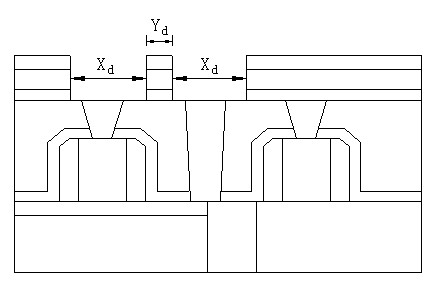
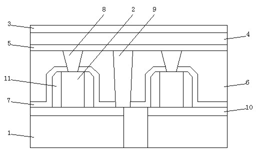
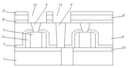
[0026] like Figure 2-7 As shown, the present invention provides a copper back-end interconnection process. In a process of 32 nanometers and below, a substrate 1 prepared by a Damascene process is provided with a gate 2 of a semiconductor device and implanted in the substrate 1. The source / drain doped region 10, and the contact hole etch barrier layer 7 covering the substrate 1 and the gate 2, covering the contact hole etch barrier layer 7 from top to bottom are sequentially provided with a first hard mask Film layer 3, metal insulating dielectric layer 4, metal etching barrier layer 5, contact hole insulating oxide layer film 6, contact hole etching barrier layer 7 partially covers source / drain doped region 10 and gate 2 on substrate 1 The upper surface of the upper surface and the upper surface and the outer surface of the gate spacer 11; wher...


PUM

PropertyMeasurementUnit
Thicknessaaaaaaaaaa
Thicknessaaaaaaaaaa
Thicknessaaaaaaaaaa

Abstract

The invention relates to the field of micro-electronics, particularly a copper subsequent interconnection technique. In the copper subsequent interconnection technique, a hard mask technology is utilized to enhance the etching resistance of the non-etching region in the subsequent etching process and reduce the drain current increase caused by the decreased thickness of the insulating material between metal conductors on the premise of keeping the chip area unchanged, thereby enhancing the yield of the device.

Description

technical field [0001] The invention relates to the field of microelectronics, in particular to a copper back-channel interconnection process. Background technique [0002] With the rapid development of nanofabrication technology, the feature size of transistors has entered the nanometer level. Improving the performance of current mainstream silicon CMOS devices through proportional reduction methods is subject to more and more physical and technological constraints. Therefore, the development of silicon technology compatible New materials and new structures have become important topics at present. [0003] With the continuous improvement of integrated circuit manufacturing technology and the continuous shrinking of line width in lithography technology, the area of ​​semiconductor devices is becoming smaller and smaller. The layout of semiconductors has evolved from ordinary single-function separation devices to integrated high-density multi-functional Integrated circuit; f...

Claims


Application Information

Patent Timeline
IPC IPC(8): H01L21/768
Inventor 朱骏张旭昇
Owner SHANGHAI HUALI MICROELECTRONICS CORP
Why Eureka
Try Eureka