
Semiconductor light emitting element and manufacturing method thereof

A technology for light-emitting elements and semiconductors, applied in semiconductor devices, electrical components, circuits, etc., can solve the problems of deterioration of the reliability of light-emitting diodes, inability to improve brightness, and temperature rise of light-emitting diodes.

Active Publication Date: 2016-04-20
EPISTAR CORP
View PDF5 Cites 0 Cited by
  • Summary
  • Abstract
  • Description
  • Claims
  • Application Information

AI Technical Summary

Problems solved by technology

If the heat inside the LED cannot be effectively dissipated, the temperature of the LED will rise, deteriorating the reliability of the LED
On the other hand, if the light generated by the light-emitting diode cannot be effectively extracted, part of the light will be reflected or refracted inside the light-emitting diode due to total reflection factors, and will eventually be absorbed by the electrode or the light-emitting layer, so that the brightness cannot be improved.

Method used


Image

  • Semiconductor light emitting element and manufacturing method thereof
  • Semiconductor light emitting element and manufacturing method thereof
  • Semiconductor light emitting element and manufacturing method thereof

Examples


Embodiment Construction

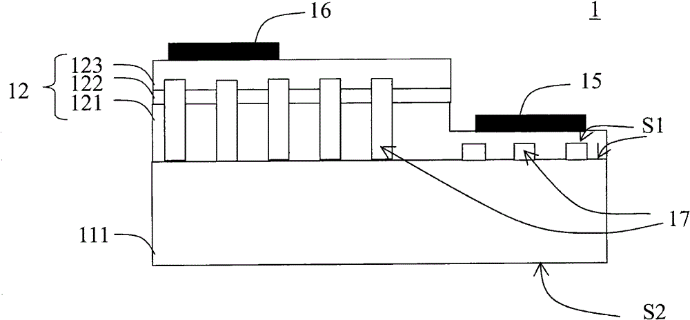
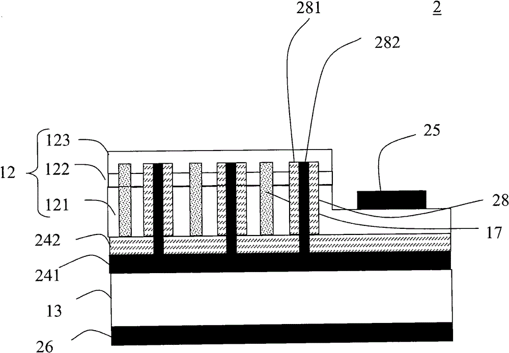
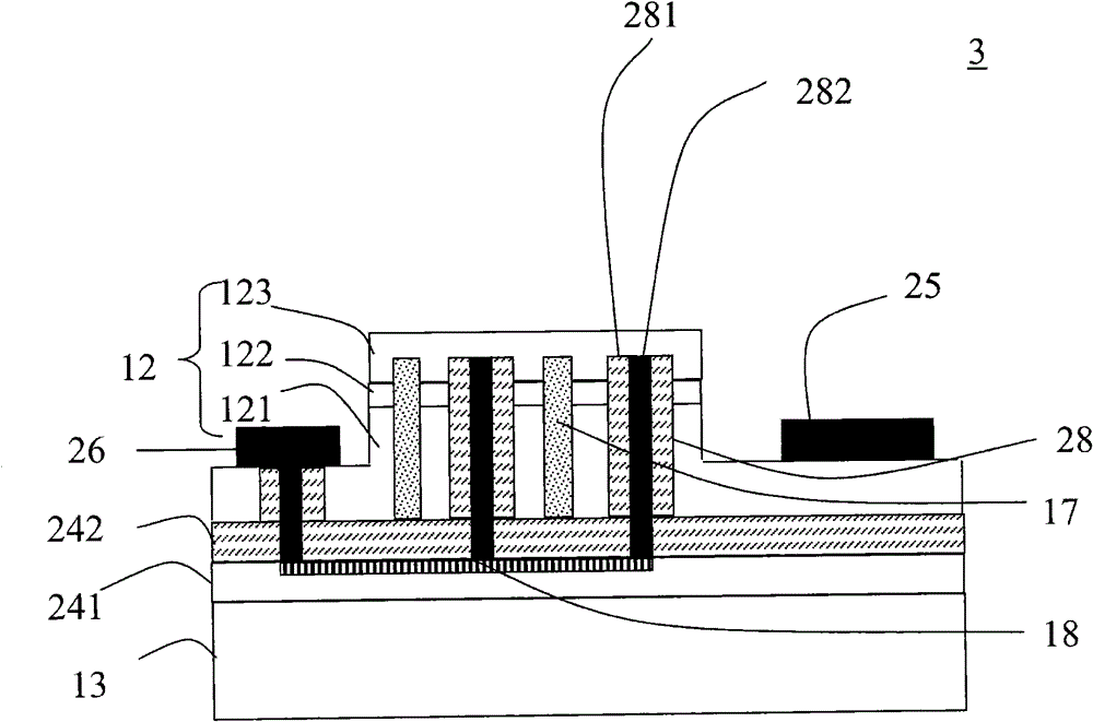
[0028] figure 1 A horizontal light-emitting element 1 according to a first embodiment of the present invention is disclosed, which includes a thinned substrate 111 with an upper surface S1 and a lower surface S2; a semiconductor light-emitting structure 12 is located on the upper surface S1 of the thinned substrate, comprising multiple layers of semiconductors layer and a plurality of first channels 17; wherein the multilayer semiconductor layer includes a first conductivity type semiconductor layer 121, an active layer 122, and a second conductivity type semiconductor layer 123, wherein a part of the first conductivity type semiconductor layer 121 A part of the semiconductor light emitting structure 12 is removed and exposed; a first wire pad 15 and a second wire pad 16 are electrically connected to the first conductive type semiconductor layer 121 and the second conductive type semiconductor layer 123 respectively, and the first The wire pads 15 and the second wire pads 16 a...


PUM


Abstract

The invention discloses a semiconductor light-emitting element and a manufacturing method thereof. The semiconductor light-emitting element comprises a semiconductor light-emitting structure and a thinned substrate, and the semiconductor light-emitting structure comprises a plurality of semiconductor layers and a plurality of first channels, wherein the first channels have special depths and penetrate through at least two semiconductor layers.

Description

technical field [0001] The present invention relates to a semiconductor light emitting element and a manufacturing method thereof, in particular to a semiconductor light emitting element with a semiconductor light emitting structure comprising multiple semiconductor layers and a plurality of first channels and a manufacturing method thereof. Background technique [0002] Semiconductor light-emitting elements, such as light-emitting diodes (LEDs), have been continuously improved in brightness in recent years, and their application fields have expanded from traditional indicator lights or decorative purposes to light sources for various devices, and even in the near future, they are likely to replace traditional The fluorescent lamp has become the light source in the field of new generation lighting. [0003] At present, the internal quantum efficiency of LEDs is about 50% to 80%; about 20% to 50% of the input power cannot be converted into light, but is generated in the LED i...

Claims


Application Information

Patent Timeline
Patent Type & Authority Patents(China)
IPC IPC(8): H01L33/02H01L33/00
Inventor 谢明勋陈威佑张利铭王健源姚久琳
Owner EPISTAR CORP
Learn More