Method and device for bad pixel compensation
A bad pixel and pixel technology, applied in the field of bad pixel compensation, can solve problems such as poor image quality, bad pixel compensation processing effect, side effects, etc., to achieve proper bad pixel compensation, good image quality, and maintain image quality Effect
- Summary
- Abstract
- Description
- Claims
- Application Information
AI Technical Summary
Problems solved by technology
Method used
Image
Examples
Embodiment Construction
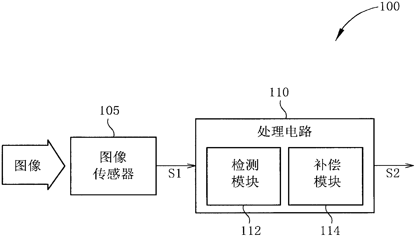
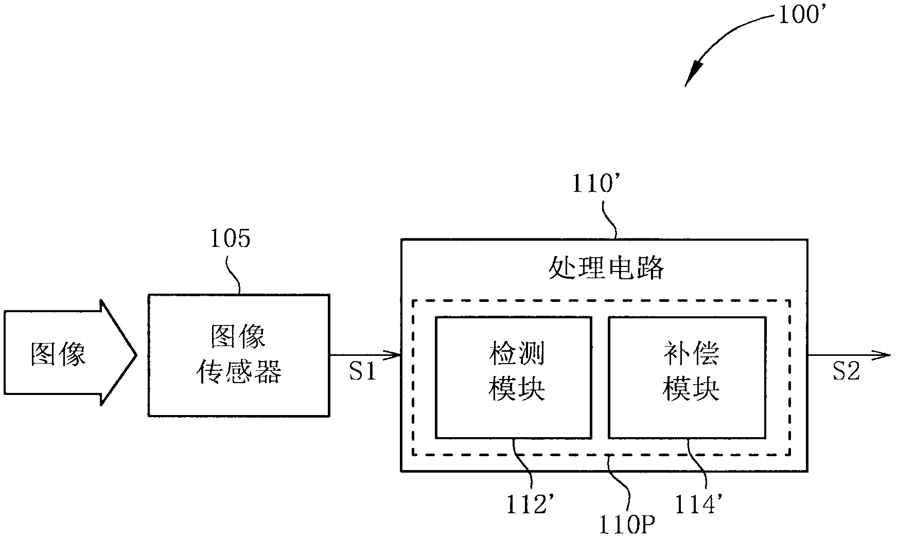
[0028] Please refer to Figure 1A , Figure 1A It is a schematic diagram of a device 100 for bad pixel compensation according to a first embodiment of the present invention. The device 100 includes an image sensor 105 and a processing circuit 110 , and the processing circuit 110 includes a detection module 112 and a compensation module 114 . According to this embodiment, the processing circuit 110 receives at least one image signal S1 representing an image from the image sensor 105 , and performs bad pixel compensation on the image, wherein the image is a Bayer pattern image. Such as Figure 1A As shown, the processing circuit 110 can output at least one image signal S2 carrying the compensated image. In addition, the detection module 112 can perform detection to generate a plurality of detection values, and the compensation module 114 can selectively perform bad pixel compensation on a target pixel according to at least a part of the detection values. During actual operation...
PUM
 Abstract
Description
Claims
Application Information


