Printed circuit board with combined type via holes

A printed circuit board, composite technology, applied in the direction of printed circuit components, electrical connection printed components, etc., can solve the problem of signal quality, affect the overall system execution efficiency and other problems, and achieve the effect of reducing impedance discontinuity

Active Publication Date: 2012-07-11
九江耀宇精密电路有限公司
View PDF5 Cites 2 Cited by
  • Summary
  • Abstract
  • Description
  • Claims
  • Application Information

AI Technical Summary

Problems solved by technology

For PCBs, the most important thing to maintain signal integrity is impedance matching and consistent continuity. When the impedance is discontinuous, it will cause signal quality problems at least, and affect the overall system execution efficiency at worst.

Method used


Image

  • Printed circuit board with combined type via holes
  • Printed circuit board with combined type via holes
  • Printed circuit board with combined type via holes

Examples


Embodiment Construction

[0058] Below in conjunction with accompanying drawing and preferred embodiment the present invention is described in further detail:

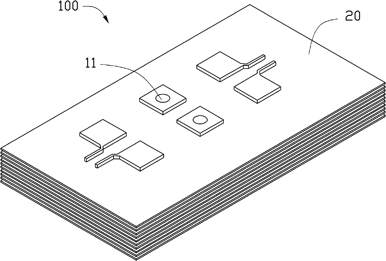
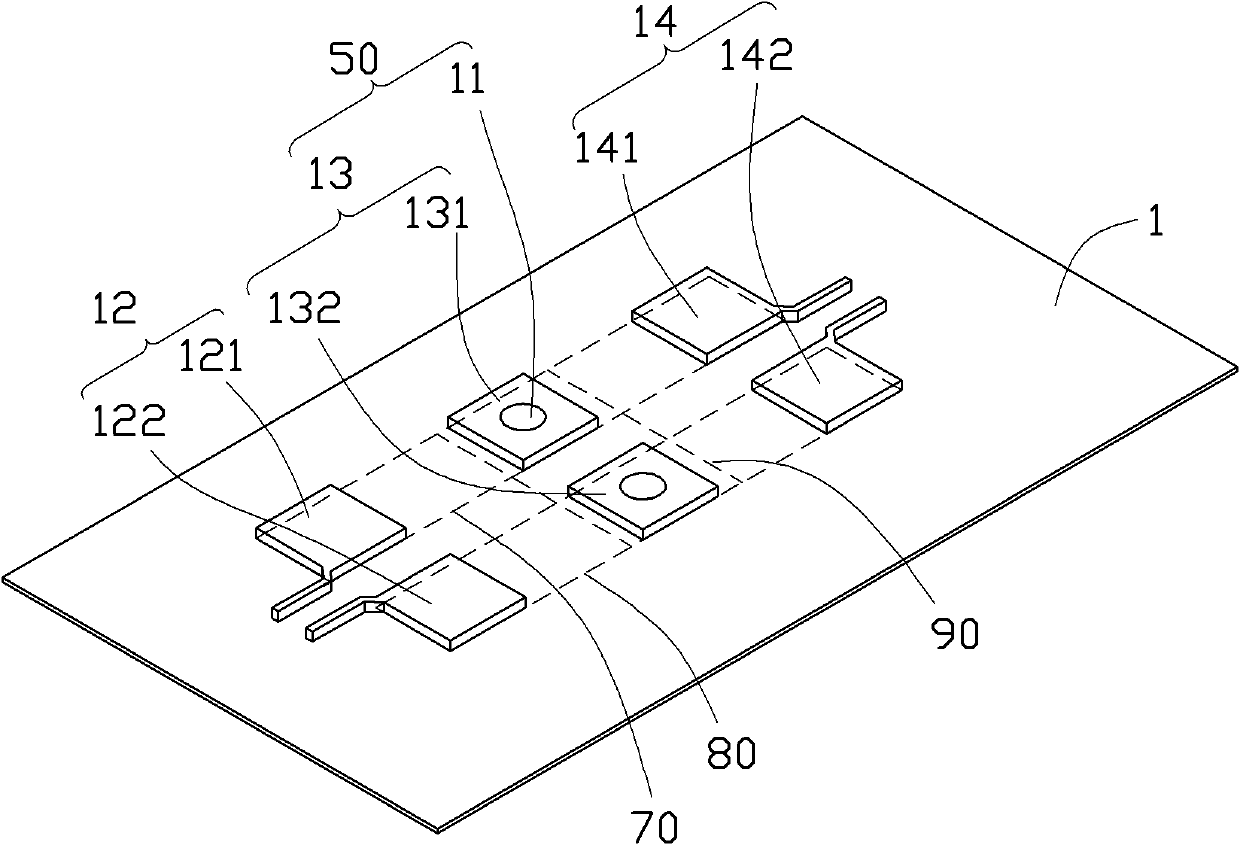
[0059] see Figure 1 to Figure 6 , the printed circuit board 100 provided with composite via holes in the present invention includes a board body 20 and a through hole 11 penetrating through each layer of the board body 20 . In this embodiment, the board body 10 is a 10-layer board body, the first layer 1, the third layer, the eighth layer and the tenth layer 10 are signal layers; the second layer 2, the fourth layer 4, the fifth layer Layer 9, sixth layer, seventh layer and ninth layer 9 are reference layers. The top of the through hole 11 is located on the first layer. The bottom of the through hole 11 is located at the tenth layer.

[0060] Please continue to refer figure 2 and image 3, first to third pairs of pads 12-14 are arranged on the first layer 1. Tops of the through holes 11 penetrate through the second pair of pads 13 . Wh...


PUM


Abstract

The invention discloses a printed circuit board with combined type via holes. The printed circuit board comprises a board body and a pair of through holes passing through the board body. The board body comprises a signal layer used as a top layer, a first reference layer adjacent to the signal layer and a second reference layer which is not adjacent to the signal layer. The signal layer is provided with a first pair of welding pads and a second pair of welding pads. The through holes pass through the first pair of welding pads and form a combined type via hole with the first pair of welding pads. A first keep-off hole is formed on the first reference layer. The first keep-off hole is corresponding to the first and second pair of welding pads on the signal layer and the combined type via hole. A second keep-off hole is formed on the second reference layer. A second keep-off hole is formed on the second reference layer, and surrounds the through holes located on the second keep-off hole. The impedance discontinuity on the printed circuit board is effectively reduced in the printed circuit board with combined type via holes.

Description

technical field [0001] The invention relates to a printed circuit board, in particular to a printed circuit board provided with composite via holes. Background technique [0002] As data communication speeds increase, signal integrity is critical for smooth data transmission. Therefore, signal integrity has become one of the factors that must be considered in the design of a printed circuit board (Printed Circuit Board, PCB). The parameters of electronic components and PCB, the layout of electronic components on PCB and other factors will affect the integrity of the signal. How to fully consider the signal integrity factor in the PCB design process and take effective control measures to reduce its impact has become a hot topic in the PCB design industry today. For PCBs, the most important thing to maintain signal integrity is impedance matching and consistent continuity. When impedance is discontinuous, it will cause signal quality problems at least, and affect the overall...

Claims


Application Information

Patent Timeline
Patent Type & Authority Applications(China)
IPC IPC(8): H05K1/11
Inventor 陈永杰李政宪谢博全许寿国严欣亭吴丹辰陈嘉琪
Owner 九江耀宇精密电路有限公司
Why Eureka
Try Eureka