Ultrasonic detachment of glass substrates from the carrier

An ultrasonic and substrate technology, which is used in the manufacture of semiconductor devices, electric solid state devices, and semiconductor/solid state devices.

Inactive Publication Date: 2016-04-27
CORNING INC
View PDF5 Cites 0 Cited by
  • Summary
  • Abstract
  • Description
  • Claims
  • Application Information

AI Technical Summary

Problems solved by technology

[0005] However, handling such thin glass substrates presents a significant technical challenge to panel manufacturers, as many production lines are not designed with the capability to handle such significantly thinner glass substrates without significant process improvements. ability

Method used


Image

  • Ultrasonic detachment of glass substrates from the carrier
  • Ultrasonic detachment of glass substrates from the carrier
  • Ultrasonic detachment of glass substrates from the carrier

Examples


Embodiment 1

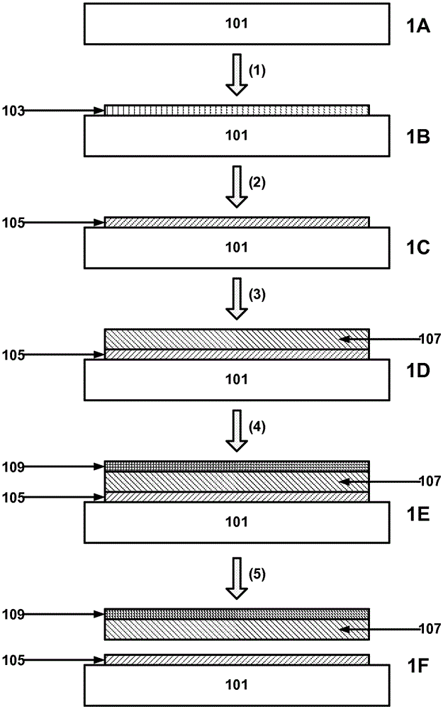
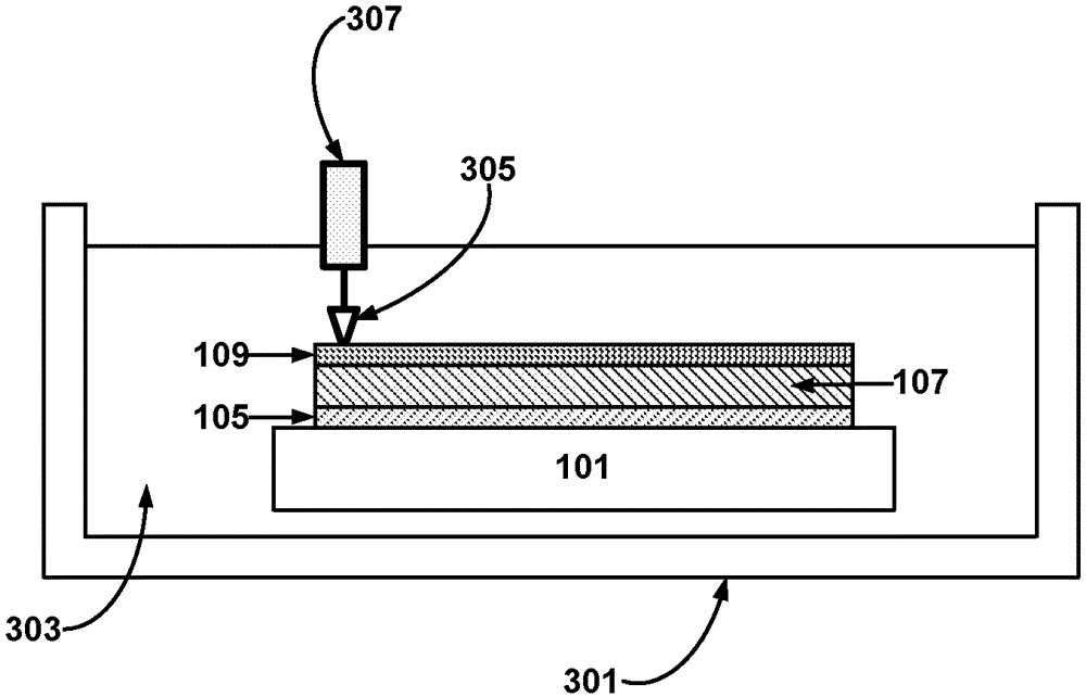
[0105] The functional substrate temporarily bonded to the carrier substrate using the fragile silica inorganic adhesive is exposed to an aggressive ultrasonic bath. Small cracks and liquid penetration into the adhesive layer were observed. This proves that exposure to ultrasound can weaken the bond between the adhesive and the functional substrate and assist in separation.

Embodiment 2

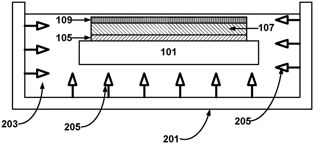
[0107] Use elastic adhesive (surface tension γS=17mJ / m 2 ) The adhesive strength of temporarily bonding the functional substrate to the carrier substrate follows figure 1 The method shown in water (surface tension γ L =72mJ / m 2 ) It is made and tested in the ultrasonic tank, and there is no malfunction. The same equipment in propanol (lower surface tension than water (γ L =23mJ / m 2 ) In the liquid), delamination was observed.


PUM

PropertyMeasurementUnit
surface roughnessaaaaaaaaaa
thicknessaaaaaaaaaa
thicknessaaaaaaaaaa

Abstract

A process for making a device comprising a thin functional substrate comprising bonding the functional substrate to a carrier substrate, forming functional components on the functional subsrate, and debonding the functional substrate from the carrier substrate by applying ultrasonic wave to the bonding interface. The application of ultrasonic wave aids the debonding step by reducing the tensile stress the functional substrate may experience.

Description

[0001] This application claims the priority rights of U.S. Application No. 12 / 548685 filed on August 27, 2009. Technical field [0002] The present invention relates to a method and apparatus for manufacturing equipment based on thin substrates. Specifically, the present invention relates to a method and apparatus for manufacturing a device on the surface of a thin substrate supported by a carrier substrate. The present invention is useful, for example, in manufacturing an optoelectronic device (for example, a display device) on the surface of a thin, flexible glass substrate with a thickness of less than 500 μm using a carrier substrate. Background technique [0003] Traditional TFTLCD displays are manufactured by forming thin film semiconductor transistors on the surface of a glass substrate. The general thickness of the glass substrate used is about 500-700 μm. LCD panel makers have made substantial capital investments in production lines for these relatively thick glass subs...

Claims


Application Information

Patent Timeline
Patent Type & Authority Patents(China)
IPC IPC(8): H01L21/68
CPCH01L21/6835B32B43/006H01L21/6836H01L2221/68327H01L2221/6835H01L2221/68381H01L2221/68395H01L2924/19041
Inventor A·R·E·卡雷S·M·加纳J·瓦库-恩辛巴
Owner CORNING INC
Why Eureka
Try Eureka