Image processing device for defect inspection and image processing method for defect inspection

An image processing device and defect inspection technology, which are applied in the field of image processing devices for defect inspection and image processing for defect inspection, and can solve problems such as practicality and difficulty in detecting and changing optical systems.

Active Publication Date: 2012-08-08
SUMITOMO CHEM CO LTD
View PDF11 Cites 28 Cited by
  • Summary
  • Abstract
  • Description
  • Claims
  • Application Information

AI Technical Summary

Problems solved by technology

Therefore, in the prior art as described above, there is a problem that it is difficult to inspect various types of defects in which the change in the path of light rays due to the defect differs at one time with sufficient accuracy.
In the defect inspection device using the dark field method, as described above, it is necessary to arrange the optical system with high precision, so it is practically difficult to change the arrangement of the optical system and the size of the light-shielding body according to the type of defect.
Therefore, in the defect inspection apparatus using the dark field method in the prior art, there is a problem in that by selecting the configuration of the optical system and the size of the light-shielding body that can detect a specific type of defect that exists in many , sometimes it is not possible to detect some types of defects with sufficient accuracy

Method used


Image

  • Image processing device for defect inspection and image processing method for defect inspection
  • Image processing device for defect inspection and image processing method for defect inspection
  • Image processing device for defect inspection and image processing method for defect inspection

Examples


Embodiment

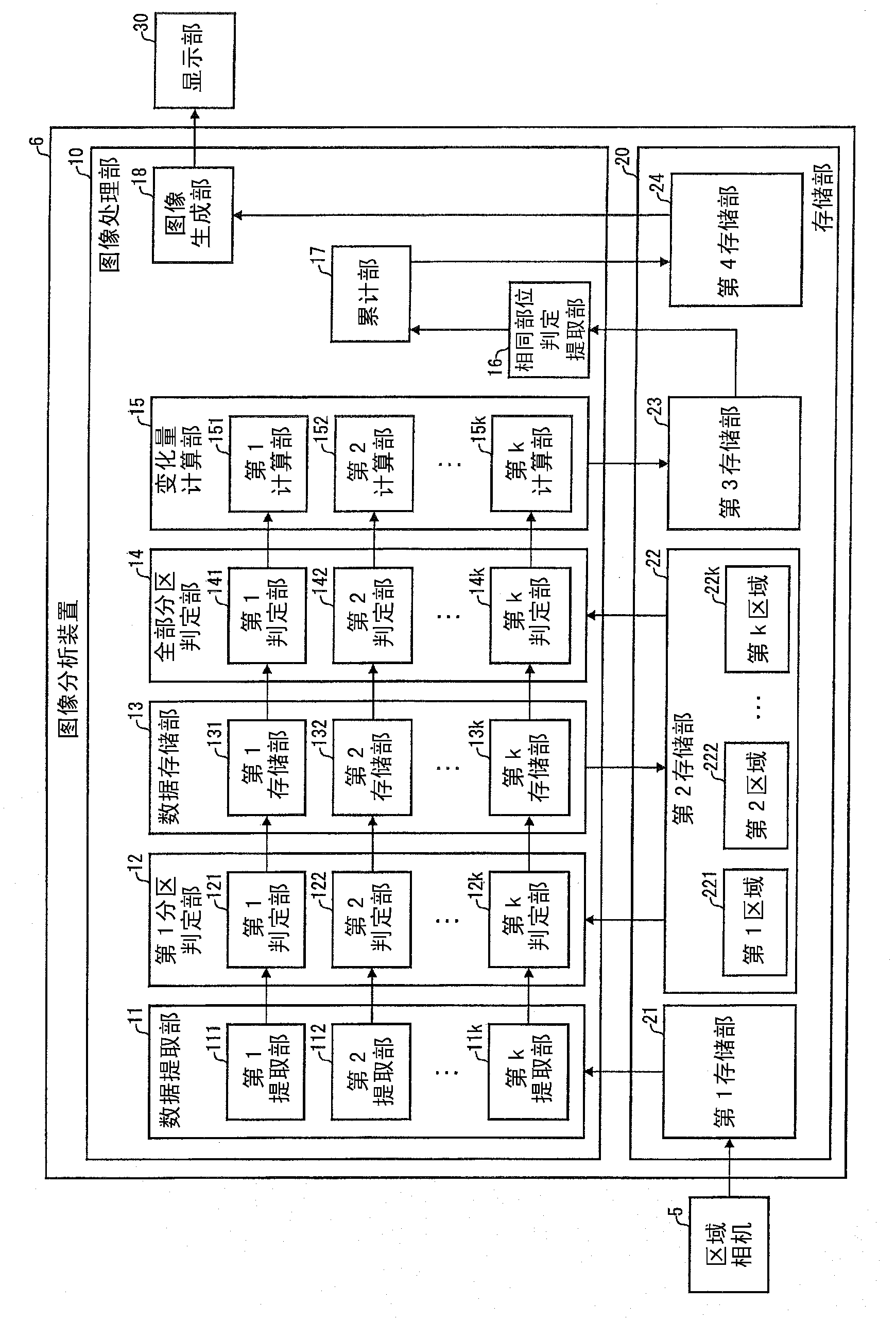
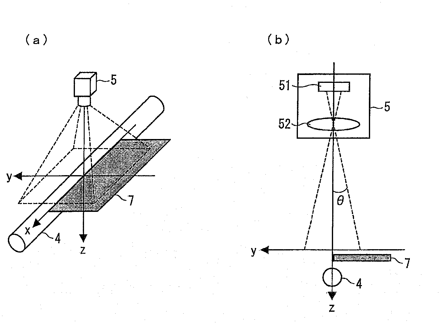
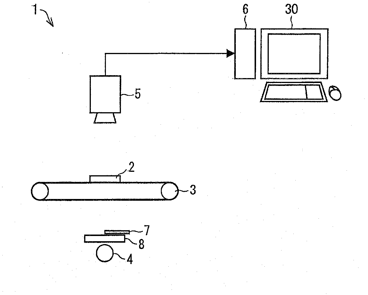
[0157] Below, the description is in image 3 An example in which RT-LCI processing is performed on image data captured by the area camera 5 in the defect inspection system 1 is shown. As the main body of the area camera 5, a double-speed progressive scan monochrome camera module (XC-HR50 manufactured by Sony Corporation) was used. In addition, as the lens of the area camera 5 , a lens manufactured by Tamuron Co., Ltd. (focal length f=35 mm) with a close-up lens of 5 mm was used. The number of pixels of the area camera 5 is 512×480 pixels, and the resolution per pixel is 70 μm / pixel. The focus of the area camera 5 is aligned with the surface of the object to be inspected. The frame rate of the area camera 5 is 60FPS, and shooting is performed in a normal TV format. RT-LCI processing was performed on 480 images taken with an area camera for 8 seconds. The conveying speed of the conveyor 3 was set at 4.2 mm / sec. That is, it is set so that the object 2 to be inspected moves 7...


PUM


Abstract

Provided are an image processing device and the like capable of detecting various kinds of defects which cause various changes in ray paths at the same time with sufficient accuracy. An image processing device (image analysis device) for defect inspection (6) processes image data obtained by temporally continuously shooting formed sheets in motion with an area camera (5), and is provided with a data extraction unit (11), a data storage unit (13), a change amount calculation unit (15), a same part judgment extraction unit (16), and an integrating unit (17). The data extraction unit (11) extracts, for a plurality of different positions on the image data, pieces of line data on the same position from different pieces of image data. The data storage unit (13) chronologically draws up the plurality of pieces of line data for each position on the image data and generates a plurality of pieces of line synthesis image data. The change amount calculation unit (15) performs differential operator computation with respect to the plurality of pieces of line synthesis image data and generates a plurality of pieces of emphasis image data. The same part judgment extraction unit (16) extracts data showing the same part of the formed sheet from the plurality of pieces of emphasis image data. The integrating unit (17) integrates luminance values of the extracted emphasis image data for each pixel and generates image data for defect inspection.

Description

technical field [0001] The present invention relates to a defect inspection system for inspecting defects of objects to be inspected such as sheets, an imaging device for defect inspection used therefor, an image processing device for defect inspection, an image processing program for defect inspection, and an image recording device for defect inspection. A computer-readable recording medium of a processing program and an image processing method for defect inspection. Background technique [0002] Generally, when inspecting defects of a sheet-shaped object to be inspected, the following method is often used: irradiating light onto the object to be inspected, and measuring and analyzing the transmitted light or reflected light to detect defects in the object to be inspected. This method is based on the configuration of the optical system of the defect inspection device, such as Figure 15 As shown, it can be roughly classified into 4 types. [0003] Figure 15 The configurat...

Claims


Application Information

Patent Timeline
Patent Type & Authority Applications(China)
IPC IPC(8): G01N21/892
CPCG06T2207/30108G06T2207/10016G01N21/892G01N21/8903G06T7/0004G01N2021/8825
Inventor 广濑修
Owner SUMITOMO CHEM CO LTD
Why Eureka
Try Eureka