Multiple-valued non-volatile memory and preparation method thereof

A memory, non-volatile technology, used in semiconductor/solid-state device manufacturing, semiconductor devices, electrical solid-state devices, etc., can solve problems such as unfavorable integration density improvement, large physical thickness, etc., to achieve low programming and erasing voltage, superior performance, reduced cost effect

Active Publication Date: 2012-09-26
INST OF MICROELECTRONICS CHINESE ACAD OF SCI
View PDF3 Cites 4 Cited by
  • Summary
  • Abstract
  • Description
  • Claims
  • Application Information

AI Technical Summary

Problems solved by technology

[0004] The present invention aims at the problem that the current non-volatile memory adopts high-k material as the storage layer and has shown good performance, but in order to achieve a certain storage window, it often needs a large physical thickness, which is not conducive to further improvement of integration density, and provides A kind of multi-valued non-volatile memory and its preparation method

Method used


Image

  • Multiple-valued non-volatile memory and preparation method thereof
  • Multiple-valued non-volatile memory and preparation method thereof
  • Multiple-valued non-volatile memory and preparation method thereof

Examples


Embodiment Construction

[0035] The principles and features of the present invention are described below in conjunction with the accompanying drawings, and the examples given are only used to explain the present invention, and are not intended to limit the scope of the present invention.

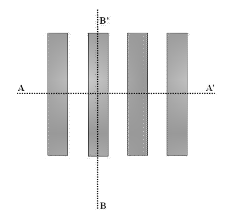
[0036] figure 1 It is a schematic diagram of the structure of the NOR memory array in two directions according to the embodiment of the present invention. Such as figure 1 As shown, the two directions of the NOR type memory array, wherein the A-A' direction is the word line direction (WL), and the B-B' direction is the bit line direction.

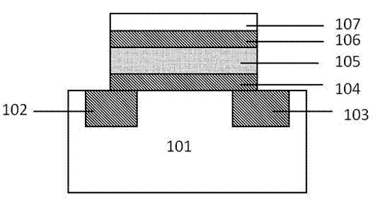
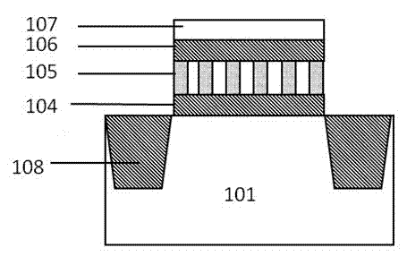
[0037] figure 2 It is a cross-sectional view of the structure of the multi-valued non-volatile memory along the direction of the bit line according to the embodiment of the present invention, image 3 It is a cross-sectional view of the structure of the multi-valued non-volatile memory along the direction of the word line according to the embodiment of the present invention. ...


PUM


Abstract

The invention relates to a multiple-valued non-volatile memory and a preparation method thereof. The memory comprises a semiconductor substrate, wherein both ends of the semiconductor substrate include a source electrode and a drain electrode respectively along the direction of a memory bit line and both ends of the semiconductor substrate include a shallow tunnel isolation structure respectively along the direction of a memory sub-line. A tunneling dielectric layer, a charge storage layer, a charge blocking layer, and a gate electrode are sequentially arranged on the semiconductor substrate, wherein the charge storage layer is a combination of two different storage materials which are alternatively arranged along the direction of the memory sub-line. The multiple-valued non-volatile memory of the invention adopts the storage layer formed by alternatively arranging the two different materials, which increases the storage density, promises a large window while reducing the thickness of a gate dielectric layer greatly,. Therefore, multiple-valued storage and high-density storage are realized the cost is reduced in turn.

Description

technical field [0001] The invention relates to a structure and a preparation method of a non-volatile memory, in particular to a multi-valued non-volatile memory with high integration density and localized charge storage and a preparation method thereof, belonging to the technical field of microelectronics manufacturing and memory. Background technique [0002] The current microelectronics products are mainly divided into two categories: logic devices and storage devices, and storage devices are needed in almost all electronic products today, so storage devices occupy a very important position in the field of microelectronics. Storage devices can generally be classified into volatile memories and non-volatile memories. The main feature of non-volatile memory is the ability to retain stored information for a long period of time without power on. It not only has the characteristics of read-only memory (ROM), but also has high access speed, and is easy to erase and rewrite, ...

Claims


Application Information

Patent Timeline
IPC IPC(8): H01L27/115H01L29/51H01L21/8247H01L21/768
Inventor 刘明许中广霍宗亮谢常青龙世兵李冬梅朱晨昕
Owner INST OF MICROELECTRONICS CHINESE ACAD OF SCI
Why Eureka
Try Eureka