Circuit board with BGA area
A technology of circuit boards and areas, applied in the direction of circuit devices, printed circuits, printed circuits, etc., can solve the problems of impedance mismatch, affecting the quality of signal transmission, and the impedance of signal lines cannot be consistent, etc.
- Summary
- Abstract
- Description
- Claims
- Application Information
AI Technical Summary
Problems solved by technology
Method used
Image
Examples
Embodiment Construction
[0015] The present invention will be further described in detail below in conjunction with the accompanying drawings.
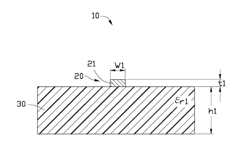
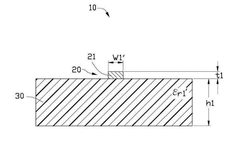
[0016] Please refer to figure 1 , figure 2 , Which discloses the circuit board 10 of the first embodiment of the present invention, wherein: image 3 Is a schematic cross-sectional view of the circuit board 10 in the non-BGA area, Figure 4 It is a schematic cross-sectional view of the circuit board 10 in the BGA area.
[0017] The circuit board 10 includes a signal wiring layer 20 and a dielectric layer 30 adjacent to the signal wiring layer 20. In practical applications, the circuit board 10 is a multilayer circuit board, which can be 4 layers, 6 layers, 8 layers, or more according to actual needs. For simplicity, in the drawings, only the signal wiring layer 20 and the dielectric layer 30 related to the present invention are shown.
[0018] The dielectric layer 30 is used to fix the signal wiring layer 20 and isolate the signal wiring layer 20 from other conduc...
PUM
 Abstract
Description
Claims
Application Information


