Crystal growth methods and systems
A crystal growth and crystal technology, applied in the field of large and high-purity crystal growth, can solve problems such as defective lattice, distortion, and low wafer yield
- Summary
- Abstract
- Description
- Claims
- Application Information
AI Technical Summary
Problems solved by technology
Method used
Image
Examples
Embodiment Construction
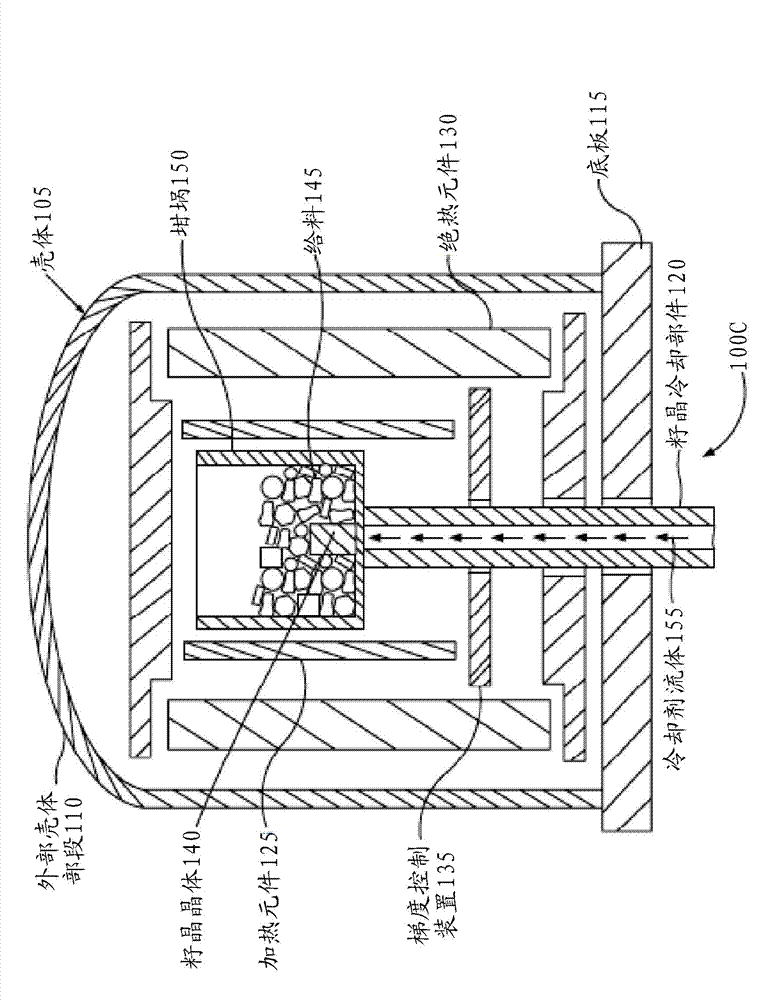
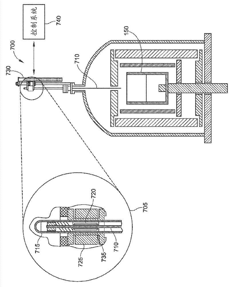
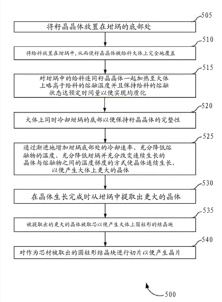
[0049] Disclosed herein is a crystal growth system and method thereof. In the following detailed description of embodiments of the invention, reference is made to the accompanying drawings, which form a part hereof and which illustrate, by way of example, specific embodiments in which the invention may be practiced. The details of these embodiments are fully disclosed herein to enable those skilled in the art to practice the invention, and it is to be understood that other embodiments may be utilized and other changes may be made without departing from the scope of the invention. Therefore, the following detailed description is not intended to be limiting, and the scope of the invention is defined by the appended claims.
[0050] The terms "larger solidified single crystal", "larger single crystal", "larger crystal" and "single crystal" are used interchangeably herein. Furthermore, the terms "convex crystal growth surface" and "crystal growth surface" are interchangeable here...
PUM
 Abstract
Description
Claims
Application Information


