Input device and display device provided with same
一种输入装置、显示装置的技术,应用在数据处理的输入/输出过程、光学、仪器等方向,能够解决第2检测电极破损等问题
- Summary
- Abstract
- Description
- Claims
- Application Information
AI Technical Summary
Problems solved by technology
Method used
Image

Examples
Embodiment approach 1
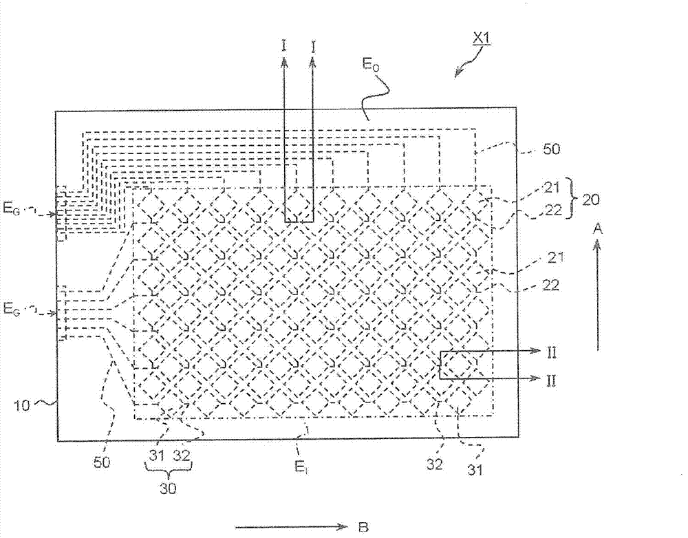
[0026] The input device X1 according to the first embodiment of the present invention will be described. The input device X1 is a capacitive touch panel.
[0027] like figure 1 As shown, the input device X1 has an input area E for inputting information by the user's finger operation or the like I , and in input area E I the outer side of the outer region E o . In addition, in the outer region E o The external conduction region E is the region that is electrically connected to the FPC (Flexible Printed Circuit) outside the figure. G .
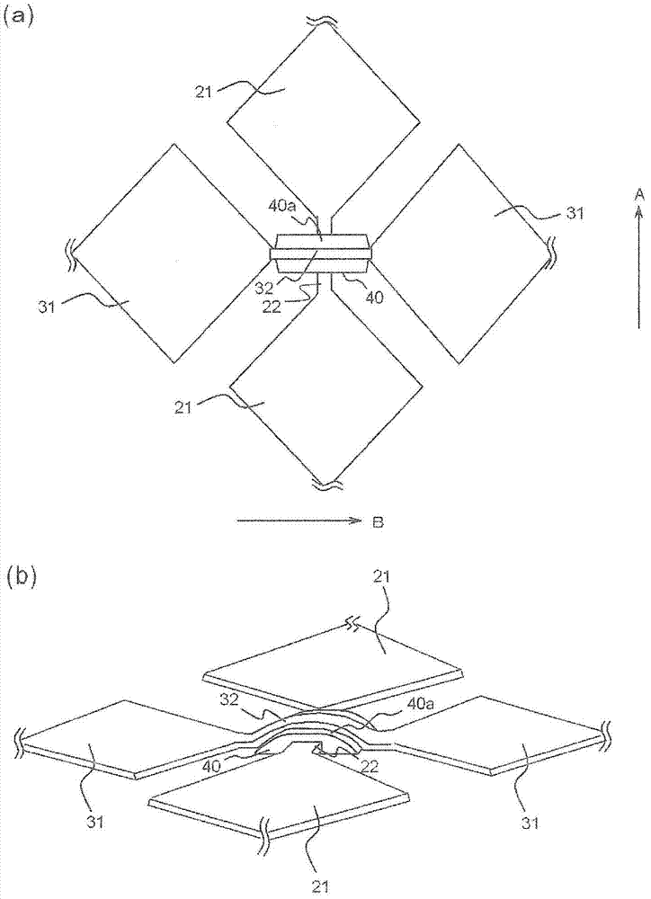
[0028] Input device X1 such as Figure 1 to Figure 4 As shown, the base body 10 , the first detection electrode pattern 20 , the second detection electrode pattern 30 , the insulator 40 , and the detection wiring 50 are provided.
[0029] base 10 such as image 3 (a) and image 3 As shown in (b), it has a main surface 10a. Although the shape in plan view of the base body 10 is, for example, a rectangular shape, it is not limited to th...
Embodiment approach 2
[0056] Next, the input device X2 according to the second embodiment of the present invention will be described. The input device X2 is, like the input device X1, a capacitive touch panel.
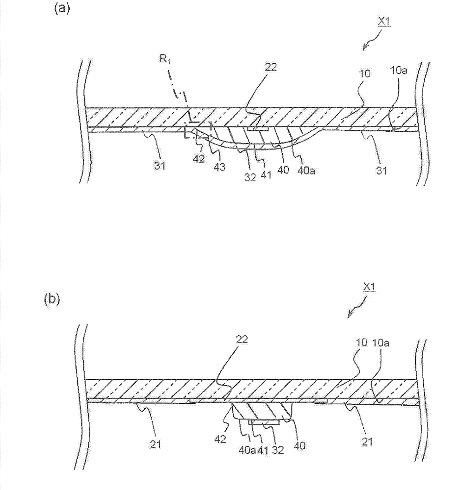
[0057] Image 6 is a diagram representing the input device X2, and is the figure 1 The I-I corresponding cross-sectional view. Figure 7 is an enlarged representation Image 6 R 2 Part of the diagram is a diagram for explaining a change in the inclination angle θ of the insulator 40 with respect to the main surface 10 a of the base body 10 . also, Figure 7 The inclination angle θ of each part of the insulator 40 is the angle formed by the tangent line and the main surface 10 a of the base body 10 when a tangent line is drawn at each part of the insulator 40 .
[0058] In the input device X2, such as Figure 7 As shown, the inclination angle θ of the insulator 40 with respect to the main surface 10a of the base body 10 has a minimum value and a maximum value between the end portion 4...
Embodiment approach 3
[0061] Next, the input device X3 according to the third embodiment of the present invention will be described. The input device X3 is, like the input devices X1 and X2, a capacitive touch panel.
[0062] Figure 8is a diagram representing the input device X3, and is the figure 1 The I-I corresponding cross-sectional view. Figure 9 is an enlarged representation Figure 8 A plan view of the main part of the input device X3.
[0063] In the input device X3, such as Figure 8 As shown, in the cross section along the second detection electrode pattern 30 , the thickness L1 of the second connection electrode 32 in the second detection electrode pattern 30 located at the end portion 42 of the insulator 40 is larger than that of the second detection electrode pattern 30 located at the top 41 of the insulator 40 Thickness L2 of the second connection electrode 32 in the electrode pattern 30 . Therefore, even if stress is applied to the second connection electrode 32 located at th...
PUM
 Abstract
Description
Claims
Application Information
 - Generate Ideas
- Intellectual Property
- Life Sciences
- Materials
- Tech Scout
- Unparalleled Data Quality
- Higher Quality Content
- 60% Fewer Hallucinations
Browse by: Latest US Patents, China's latest patents, Technical Efficacy Thesaurus, Application Domain, Technology Topic, Popular Technical Reports.
© 2025 PatSnap. All rights reserved.Legal|Privacy policy|Modern Slavery Act Transparency Statement|Sitemap|About US| Contact US: help@patsnap.com