Stack semiconductor package formed by multiple molding and method of manufacturing the same

a technology of stack semiconductor and multiple molding, which is applied in the direction of semiconductor devices, semiconductor/solid-state device details, electrical devices, etc., can solve the problems of easy breakage of conventional stack semiconductor packages, and achieve the effect of preventing breakag

Inactive Publication Date: 2009-01-13
SAMSUNG ELECTRONICS CO LTD
View PDF9 Cites 115 Cited by
  • Summary
  • Abstract
  • Description
  • Claims
  • Application Information

AI Technical Summary

Benefits of technology

[0009]In one aspect, the present invention provides a stack semiconductor package formed by multiple molding that can prevent breakage by dispersing stress that tends to concentrate at a connecting portion between discrete semiconductor packages. In another aspect, the present invention provides a method of manufacturing the stack semiconductor package using multiple molding.

Problems solved by technology

However, the conventional stack semiconductor package is susceptible to breakage due to stress concentration at a connecting portion A between the first and second semiconductor packages 20 and 40 in response to changes in the external environment and conditions.

Method used


Image

  • Stack semiconductor package formed by multiple molding and method of manufacturing the same
  • Stack semiconductor package formed by multiple molding and method of manufacturing the same
  • Stack semiconductor package formed by multiple molding and method of manufacturing the same

Examples


first embodiment

[0018]FIGS. 2-10 are cross-sectional views illustrating a method of manufacturing a stack semiconductor package using multiple molding according to a first embodiment of the present invention.

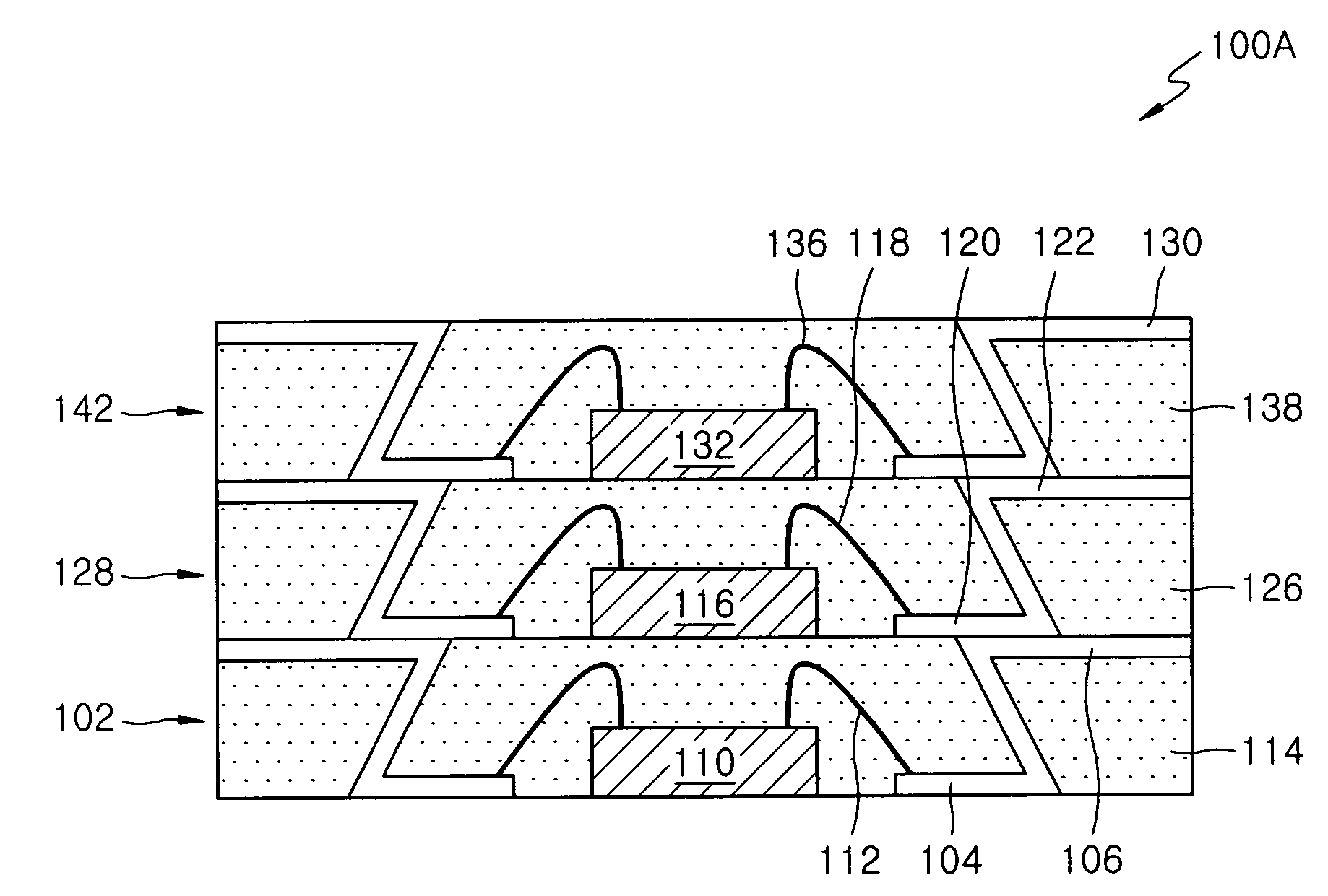
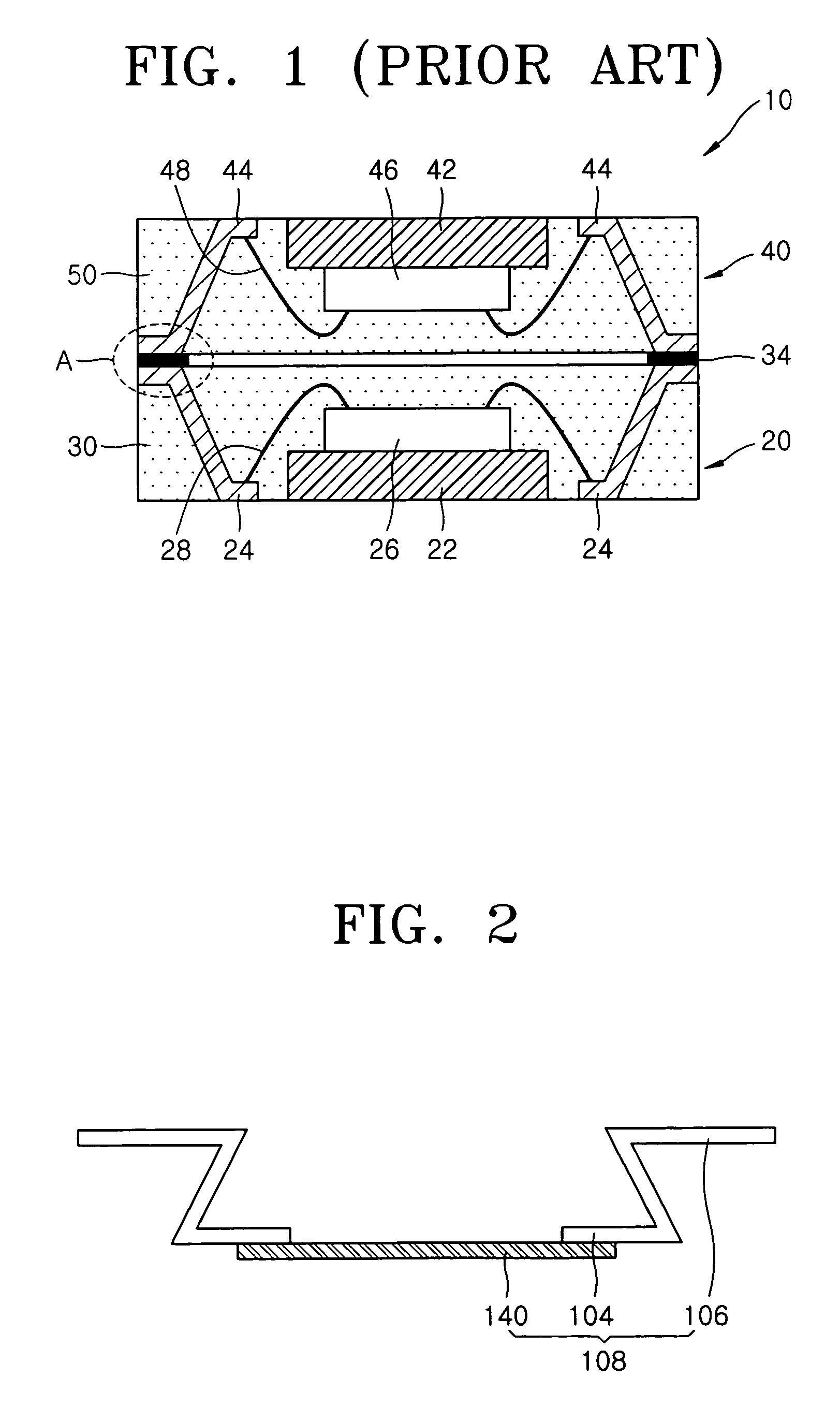
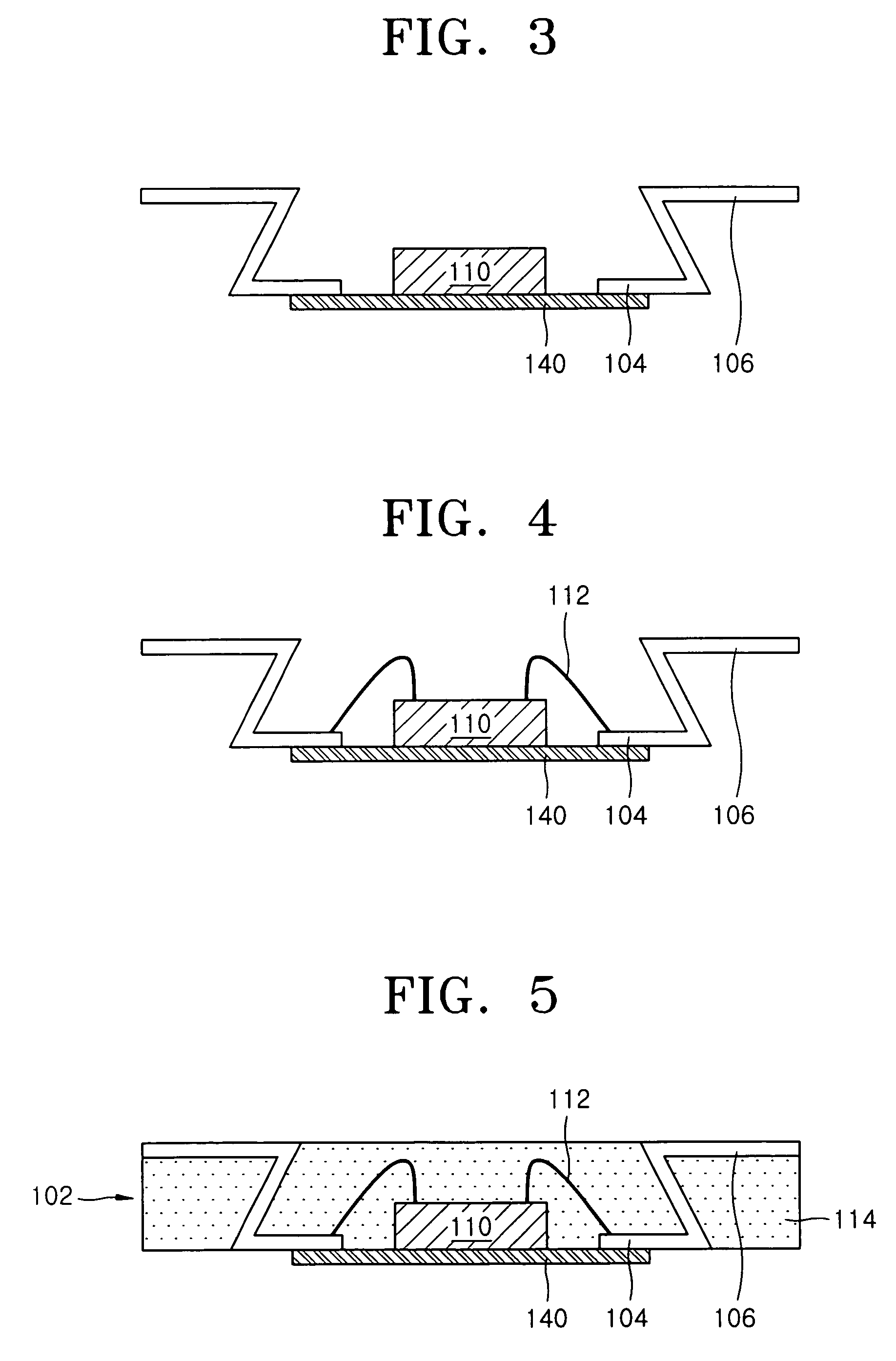
[0019]Referring to FIG. 2, a first Z-shaped leadframe 108 is prepared. The first leadframe 108 includes first leads 104, which may be connected with first wires 112 (FIG. 4) in a first semiconductor package 102 (FIG. 7), second leads 106 extending upward from of the first leads 104, and a tape 140 attached to the bottom surfaces of the first leads 104. A portion of the second lead 106 may be exposed even after the first semiconductor package 102 is molded. When a plurality of semiconductor packages are stacked, the second leads 106 provide an electrical path through which the plurality of semiconductor packages are electrically connected to one another. For example, the top surfaces of the second leads 106 in the lead frame 108 can be electrically connected to the bottom surfaces of the first l...

second embodiment

[0029]FIGS. 11 and 12 are cross-sectional views illustrating a method of manufacturing a stack semiconductor package 200A using a multiple molding technique according to a second embodiment of the present invention. While the leadframes in the stack semiconductor package 100A are Z-shaped, it may have various other shapes like the shape of the first leadframe 208 shown in FIG. 11. Additionally, the first lead 204 may have various other shapes to allow wire bonding to the first semiconductor chip 210 and to allow the tape 240 to extend between the leadframes 208. The second lead 206 may also have any variety of shapes such that it can connect to the first lead204 and extend upwards.

[0030]Referring to FIG. 12, a first semiconductor package 202 is manufactured according to the same or similar method as in the first embodiment using the first leadframe 208. Subsequently, second and third semiconductor packages 228 and 242 are sequentially manufactured by multiple molding using second se...

third embodiment

[0033]FIGS. 13-18 are cross-sectional views illustrating a method of manufacturing a stack semiconductor package 300 using multiple molding according to a third embodiment of the present invention.

[0034]While the first and second embodiments use a separate leadframe for each semiconductor package, the present embodiment uses a common leadframe 308 for a stack semiconductor package including two semiconductor packages.

[0035]Referring to FIG. 13, the common leadframe 308 includes first and second leads 304 and 306 connected in a stepped pattern. A tape 340 is attached to the top surfaces of the second leads 306 and provides a space for mounting a first semiconductor chip. The first and second leads 304 and 306 will be connected to first and second wires.

[0036]Referring to FIGS. 14-18, after a first semiconductor chip 310 is mounted on the tape 340 of the common leadframe 308, bond pads (not shown) of the first semiconductor chip 310 are coupled to the first leads 304 by, for example, ...


PUM


Abstract

Provided are a stack semiconductor package manufactured by multiple molding that can prevent the breakage due to stress concentration at a connecting portion between separate semiconductor packages and a method of manufacturing the same. The stacked semiconductor packages are combined together through sealing resins by molding them multiple times, resulting in uniform stress distribution across substantially the entire interface between the semiconductor packages.

Description

CROSS-REFERENCE TO RELATED PATENT APPLICATION[0001]This application claims the benefit of Korean Patent Application No. 10-2005-0018135, filed on Mar. 4, 2005, in the Korean Intellectual Property Office, the disclosure of which is incorporated herein in its entirety by reference.BACKGROUND OF THE INVENTION[0002]1. Field of the Invention[0003]The present invention relates to a semiconductor package and a method of manufacturing the same, and more particularly, to a vertically stacked semiconductor package with improved physical strength and a method of manufacturing the same.[0004]2. Description of the Related Art[0005]As semiconductor devices are used in a wider range of application fields, the importance of semiconductor packages that protect semiconductor chips from mechanical damage and extend their functions to the outside has significantly increased. Semiconductor packages come in various shapes and with various characteristics.[0006]Stack semiconductor packages are designed so...

Claims


Application Information

Patent Timeline
Patent Type & Authority Patents(United States)
IPC IPC(8): H01L23/02
CPCH01L21/565H01L21/568H01L21/6835H01L23/49506H01L23/49551H01L23/49575H01L24/83H01L25/0657H01L25/105H01L25/50H01L24/29H01L25/03H01L2224/48091H01L2224/48247H01L2224/8385H01L2225/0651H01L2924/01079H01L2924/01082H01L2924/07802H01L2924/18301H01L2924/00014H01L24/48H01L2224/2919H01L2924/01033H01L2924/014H01L2924/0665H01L2924/00H01L2224/45144H01L2924/181H01L24/45H01L2924/18165H01L2224/05599H01L2924/00012H01L23/52
Inventor KIM, HYUN-KI
Owner SAMSUNG ELECTRONICS CO LTD
Why Eureka
Try Eureka