Organic light-emitting diode (OLED) packaging structure, manufacturing method thereof and luminescent device

A technology of packaging structure and manufacturing method, which is applied in the manufacture of semiconductor devices, electric solid-state devices, semiconductor/solid-state devices, etc., can solve the problems of OLED observation angle dependence, achieve the effect of reducing observation angle dependence and enhancing the ability to scatter light

Active Publication Date: 2012-12-19
BOE TECH GRP CO LTD
View PDF2 Cites 16 Cited by
  • Summary
  • Abstract
  • Description
  • Claims
  • Application Information

AI Technical Summary

Problems solved by technology

The microcavity effect will cause the electroluminescence spectrum of OLED to change with the observation angle, resulting in the observation angle dependence problem of OLED

Method used


Image

  • Organic light-emitting diode (OLED) packaging structure, manufacturing method thereof and luminescent device
  • Organic light-emitting diode (OLED) packaging structure, manufacturing method thereof and luminescent device
  • Organic light-emitting diode (OLED) packaging structure, manufacturing method thereof and luminescent device

Examples


Embodiment Construction

[0044] In order to enable those skilled in the art to better understand the technical solutions of the present invention, the OLED packaging structure, manufacturing method and light-emitting device provided by the present invention will be described in detail below in conjunction with the accompanying drawings.

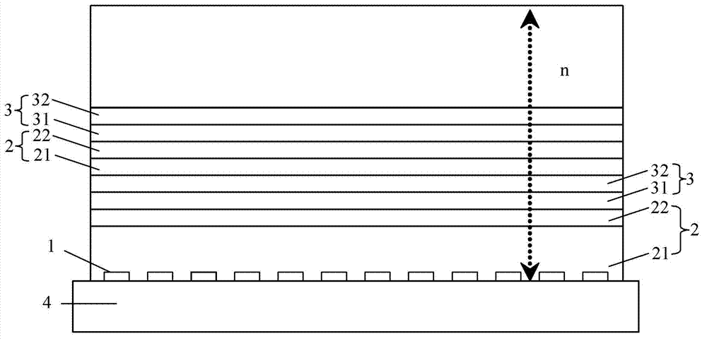
[0045] figure 1 This is a schematic structural diagram of an OLED packaging structure provided by Embodiment 1 of the present invention, such as figure 1 As shown, the OLED packaging structure may include: a base substrate 4, an OLED 1, a barrier layer 2 and an optical modulation layer 3, and the barrier layer 2 and the optical modulation layer 3 are alternately formed on the OLED 1.

[0046] In this embodiment, preferably, the barrier layer 2 and the optical modulation layer 3 can be alternately formed on the OLED 1 according to the number of alternating periods, and the optical modulation layer 3 is located on the barrier layer 2 in each alternating period. That is, on t...


PUM


Abstract

The invention discloses an organic light-emitting diode (OLED) packaging structure, a manufacturing method thereof and a luminescent device. The OLED packaging structure comprises a substrate, OLEDs, blocked layers and optical modulation layers. The OLEDs are formed on the substrate. The blocked layers and the optical modulation layers are alternately formed on the OLEDs. According to the technical scheme of the OLED packaging structure and the manufacturing method thereof, the blocked layers and the optical modulation layers are alternately formed on the OLEDs, and by the optical modulation layers, the scattering light-emitting capability of the OLEDs is enhanced, and the propagation direction of a part of light is changed, so that the observation angle dependence of the OLEDs caused by a micro-cavity effect is reduced.

Description

Technical field [0001] The invention relates to the field of organic electroluminescence display manufacturing, in particular to an OLED packaging structure and a manufacturing method thereof, and a light-emitting device. Background technique [0002] Organic Light-Emitting Diode (Organic Light-Emitting Diode, hereinafter referred to as: OLED) is called the first because of its active light emission, good temperature characteristics, low power consumption, fast response, flexibility, ultra-light and thin, and low cost. Three generations of fantasy display technology. At present, driven by the continuous capital investment and technological research and development of global manufacturers, OLED flat panel display technology is trending towards a stage of increasing maturity of mass production technology and rapid market demand. [0003] OLEDs can be divided into three types according to the direction of light emission, namely: bottom-emitting OLED, top-emitting OLED and double-side...

Claims


Application Information

Patent Timeline
Patent Type & Authority Applications(China)
IPC IPC(8): H01L51/52H01L51/56
CPCH01L51/5256H01L51/5275H10K50/8445H10K50/854H10K50/858H01L33/52H01L33/58H10K50/84H10K50/844H10K71/00
Inventor 朱儒晖于军胜
Owner BOE TECH GRP CO LTD
Why Eureka
Try Eureka