AI technical title is built by Patsnap AI team. It summarizes the technical point description of the patent document.
A technology of electronic balance and computing device, which is applied in the field of silicon chip automatic counting device
Active Publication Date: 2013-03-27
ZHEJIANG COWIN ELECTRONICS
View PDF6 Cites 5 Cited by
Summary
Abstract
Description
Claims
Application Information
AI Technical Summary
This helps you quickly interpret patents by identifying the three key elements:
Problems solved by technology
Method used
Benefits of technology
Problems solved by technology
[0006] In the actual production process, especially in the shipment inspection process, the check of the number of pieces is very important. The traditional manual spotting cannot meet the high requirements of the existing production for product quality. The photoelectric spotting machine is used in the semiconductor silicon wafer manufacturing industry. Apps have inherent flaws that cannot be avoided
Method used
Image
Click on the blue label to locate the original text in one second.
Reading with bidirectional positioning of images and text.
Examples
Embodiment 1
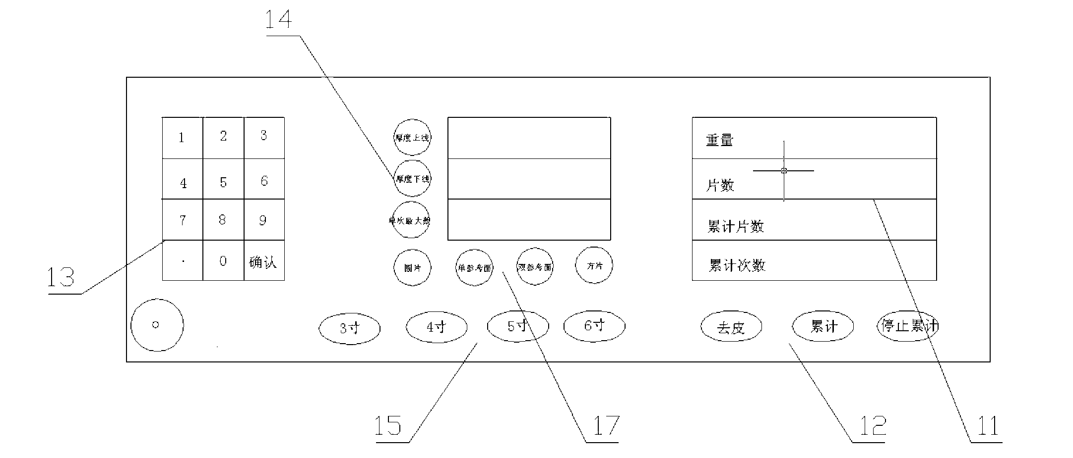
[0044] The actual use steps of the present invention: (with 285-290, 3-inch circular silicon wafers, 211pcs waiting for confirmation. According to the principle, the single maximum count n=56.)
[0045] 1. Turn on the switch of the device, and place the basket containing silicon wafers on the balance.
[0046] 2. When the display is stable, click Tare.
[0047] 3. Place the test weight on the basket and confirm that the weight display is consistent with the weight identification.
[0048] 4. Enter the silicon wafer thickness 285-290, and select "3 inches", "wafer".
[0049] 5. Put the wafers to be counted into the basket in batches, and click "Accumulate".
[0050] 6. If too many pieces are put in at one time, it will display "Exceeded" and will not be included in the cumulative number of pieces.
[0051] 7. Repeat steps 5-6 to get the final total number of pieces. Get "over", "56", "55", "over", "55", "45", respectively.
[0052] 8. "Accumulated number of pieces" display...
Embodiment 2
[0055] Shipment inspection, N14, 295-300 microns, 501pcs, wafers, 1pcs filter paper every 50pcs interval, of which 1 knife silicon wafer is 51pcs, the final inspection uses the device of the present invention for full inspection, and the final inspection requires 500pcs / box, 50pcs / Knife.
[0056] The inspection is as follows:
[0057] Testing frequency
Embodiment 3
[0059] 5-inch single reference surface, asymmetric chamfered silicon wafer, thickness 525-530 microns. The number of slices is unknown, and the number of slices is calculated using the device and method of the present invention.
[0060] 1. Input the upper and lower lines of the thickness to get the single maximum count value n=104pcs.
[0061] 2. Select the size "5 inches", "single reference plane", and press "cumulative" to count.
[0062] 3. Divided into multiple counts, respectively "52", "46", "68", "42", "45", a total of 253pcs.
[0063] 4. Checked by manual counting method, it is 253pcs, which is consistent with the result of the counting device.
PUM
Abstract
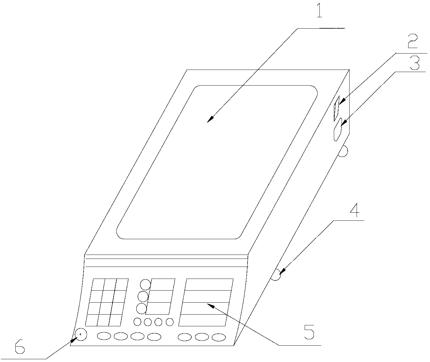
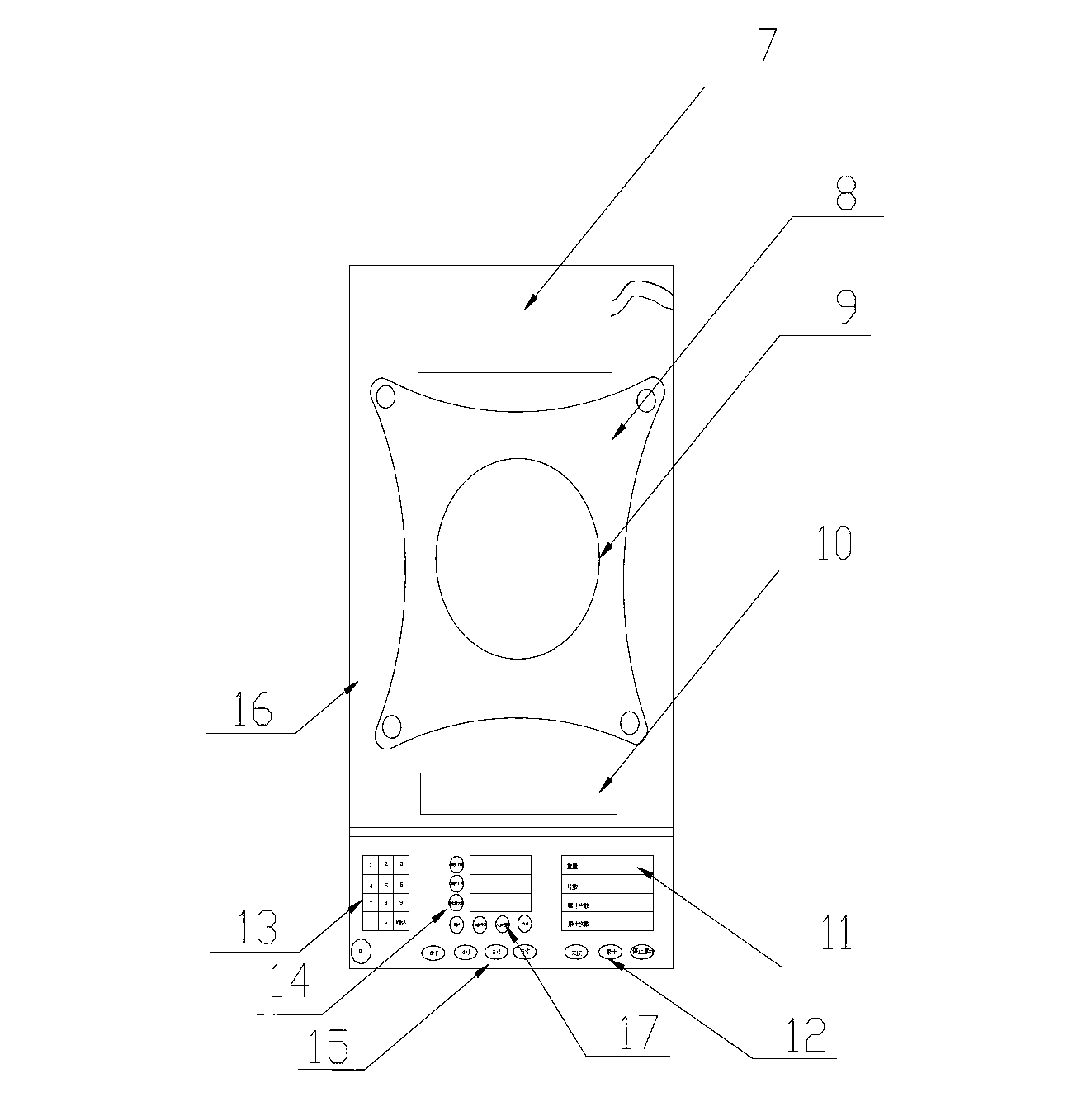
The invention discloses an electronic-balance-based automatic siliconwafer counter which comprises an electronic balance. The electronic balance comprises an input and display panel. An internal signalprocessing device is disposed in the electronic balance. The input and display panel is provided with a numeric input device, a siliconwafer thickness selection and display device, a siliconwafer specification selector, a silicon wafer size selector and a counting result display device. The counting result display device is provided with a 'weight' display panel and a 'number' display panel. The internal signalprocessing device processes input from the numeric input device, the silicon wafer thickness selection and display device, the silicon wafer specification selector and the silicon wafer size selector, and displays the silicon wafer weight and number counting result on the 'weight' display panel and the 'number' display panel. The electronic-balance-based automatic silicon wafer counter is developed based on a common electronic balance, is effective in counting silicon wafers and has the advantages of convenience, practicality and low cost.
Description
technical field [0001] The invention belongs to the field of semiconductor silicon wafer processing and manufacturing in the integrated circuit support industry, and in particular relates to an electronic balance-based automatic silicon wafer counting device, which is suitable for weighing and counting semiconductor silicon wafers. Background technique [0002] The semiconductor silicon wafer manufacturing industry belongs to the integrated circuit support industry. It has always been a key support industry and a strategic emerging industry. However, the statistics of the number of semiconductor silicon wafers have long been completed by manual spotting. Manual spotting is inevitable. Data errors will occur. In the semiconductor industry, which is an extremely rigorous field of production, the number of chips will greatly affect the product image; it will also have an adverse effect on the traceability of production data; loss. [0003] Photovoltaic industry is a rapidly de...
Claims
Application Information
Patent Timeline
Application Date:The date an application was filed.
Publication Date:The date a patent or application was officially published.
First Publication Date:The earliest publication date of a patent with the same application number.
Issue Date:Publication date of the patent grant document.
PCT Entry Date:The Entry date of PCT National Phase.
Estimated Expiry Date:The statutory expiry date of a patent right according to the Patent Law, and it is the longest term of protection that the patent right can achieve without the termination of the patent right due to other reasons(Term extension factor has been taken into account ).
Invalid Date:Actual expiry date is based on effective date or publication date of legal transaction data of invalid patent.

