Check patentability & draft patents in minutes with Patsnap Eureka AI!

High Dynamic Range Subsampling Architecture

A high dynamic range and state-of-the-art technology, applied in TV, color TV parts, TV system parts, etc., can solve problems such as full well

Active Publication Date: 2016-06-15
OMNIVISION TECH INC
View PDF3 Cites 0 Cited by
  • Summary
  • Abstract
  • Description
  • Claims
  • Application Information

AI Technical Summary

Problems solved by technology

Current charge-coupled devices (CCDs) and CMOS sensors cannot achieve this range due to full well limitations and noise floor limitations typically around 60~70dB

Method used


Image

  • High Dynamic Range Subsampling Architecture
  • High Dynamic Range Subsampling Architecture
  • High Dynamic Range Subsampling Architecture

Examples


Embodiment approach

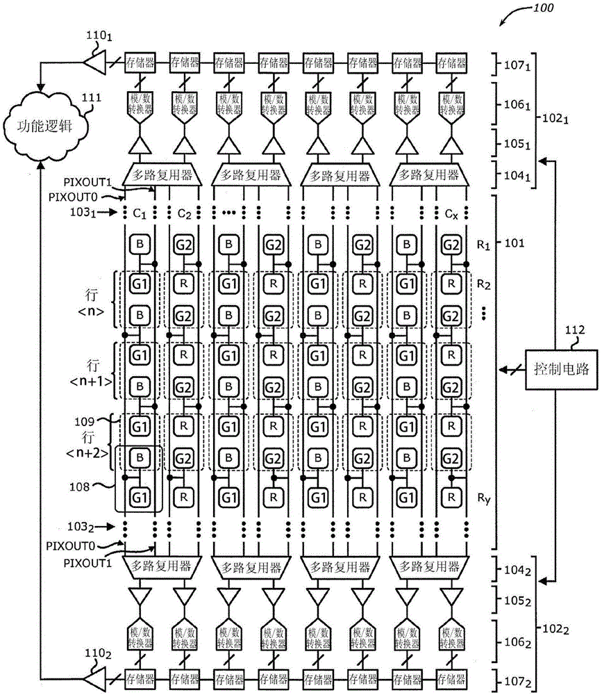
[0072] Pixel implementation, row drivers and timing

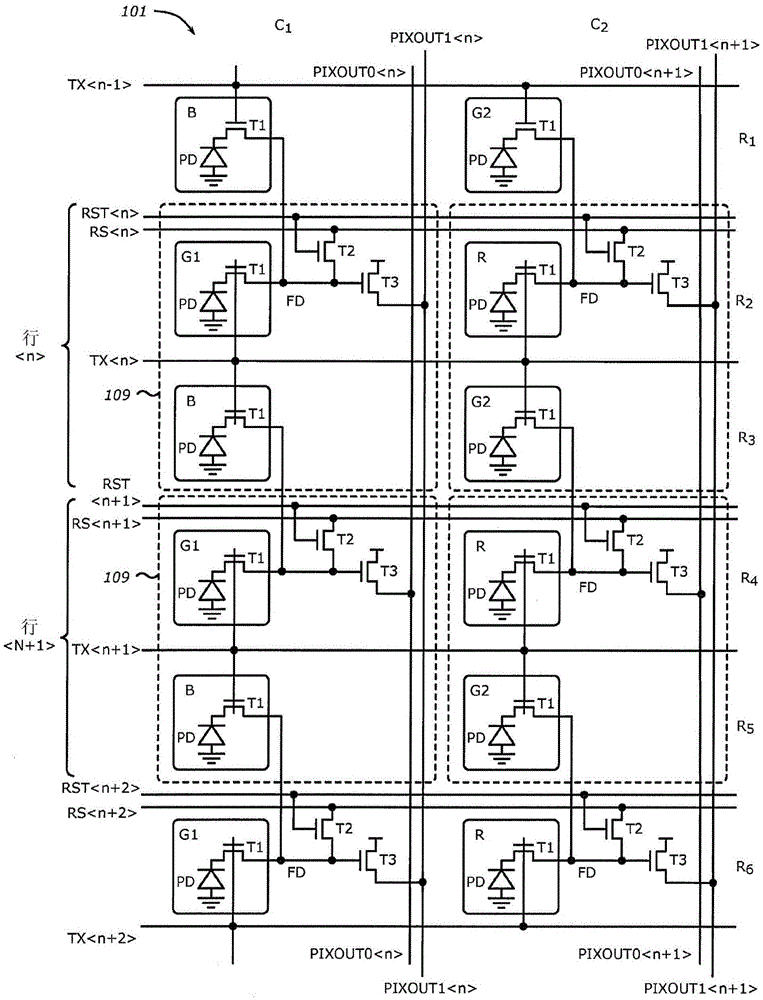
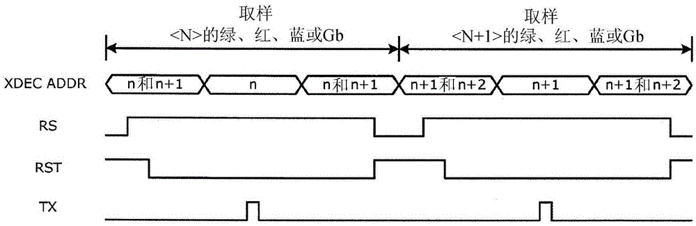
[0073] figure 2 An example of a pixel array in a multi-line simultaneous readout scheme according to an embodiment of the present invention will be described. in figure 2 In the embodiment in, two shared no-line selection pixels are used as an example. In another embodiment, other pixel structures and variations can be used. A logical unit cell 109 (enclosed by a dashed line) contains two pixels that have the same row decoder address (for example, row ) And share the same row of driver signals, the same transmission (TX) line, and the same reset (RST) and set (RS) signals.

[0074] in figure 2 , The pixels are arranged in two columns (for example, columns C1 and C2) and six rows (for example, rows R1, R2...R6). The illustrated embodiment of each pixel circuit includes a photodiode PD, a transfer transistor T1, a reset transistor T2, and a select transistor T3. During operation, the transfer transistor T1 receives the tran...


PUM


Abstract

The present invention describes a method of implementing a high dynamic range interval algorithm in an image sensor comprising a pixel array with a first super row having a first integration time and a second super row having a second integration time. The method begins by reading out image data from the first super row into a counter. Image data from the first super row is multiplied by a factor to obtain multiplied data. The factor is a ratio between the first integration time and the second integration time. The multiplied data is then compared with predetermined data. Image data from the second super row is read out into the counter. If the multiplied data is greater than the predetermined data, the multiplied data from the first super row is stored in the counter. If not, store the image data from the second super row. Other embodiments are also described.

Description

[0001] Cross reference of related applications [0002] This application claims the priority of U.S. Provisional Application No. 61 / 545,993 filed on October 11, 2011 under 35 U.S.C. 119(e), which is specifically incorporated herein by reference in its entirety. Technical field [0003] Embodiments of the present invention generally relate to a system, method, and device that implement a multi-line simultaneous readout scheme for a high-speed CMOS image sensor with backside illumination. Another embodiment of the present invention generally relates to a system, method, and device that implement a high dynamic range sub-sampling architecture. Yet another embodiment of the present invention generally relates to a system, method, and device that implement an arithmetic counter circuit for a high-performance CMOS image sensor. Background technique [0004] High-speed image sensors have been widely used in many applications in different fields, including the automotive field, machine vis...

Claims


Application Information

Patent Timeline
Patent Type & Authority Patents(China)
IPC IPC(8): H04N5/355H04N5/3745H04N5/378
CPCH04N25/531H04N25/46H04N25/57H04N25/77H04N25/75
Inventor 莫要武徐辰瞿旻骆晓东吴东晖
Owner OMNIVISION TECH INC
Features
  • R&D
  • Intellectual Property
  • Life Sciences
  • Materials
  • Tech Scout
  • Unparalleled Data Quality
  • Higher Quality Content
  • 60% Fewer Hallucinations
Learn More